
We are JHYPCB, a PCB manufacturer in China providing PCB prototypes, volume PCB production, and PCB assembly services. In the first part of this overview, we introduced the MI, material cutting, and drilling steps of the PCB production process. In the second part, we covered copper plating and circuit imaging. In the third part, we discussed pattern plating and automated optical inspection (AOI). In the fourth part, we went over solder masking, legend printing, and surface finishes.
Now in the fifth part of the PCB manufacturing process, we will explain the final stages – testing, routing, V-scoring, quality control, and shipping. After the surface finishes are applied, each printed circuit board goes through comprehensive testing using flying probe and fixture-based testers to validate full compliance with the design files. Boards then proceed to routing, which is the process of cutting the panels into individual PCBs by precision milling along the board outlines. V-scoring further prepares the boards for separation by cutting partial depth lines in between circuits.
Once routing and V-scoring are complete, each board goes through final quality control inspections, including visual, electrical, and dimensional checks. Boards that pass these inspections are then packed and shipped to customers worldwide via air or sea freight. We have a streamlined shipping process to ensure timely delivery across the globe. This concludes the full overview of our end-to-end PCB fabrication capabilities. Please reach out if you have any other questions!
Related Reading:
- Navigating the PCB Manufacturing Process Part 1: Unveiling MI, Cutting, and Drilling
- Navigating The PCB Manufacturing Process Part 2: Copper Plating, Routing
- Navigating The PCB Manufacturing Process Part 3: Pattern And AOI
- Navigating The PCB Manufacturing Process Part 4: Solder Mask, Silkscreen, Surface Finish
Step 10: Testing
In the 6th process step, we performed AOI (automated optical inspection) on the boards, mainly conducting visual inspections from the exterior side for defects like open circuits, short circuits, discontinuities, etc. However, AOI cannot detect issues with the vias and holes, such as whether there is copper inside the holes, the copper quality, or if they electrically connect properly. The next process step addresses these limitations.
We will introduce two testing methods: flying probe testing and fixture-based testing.
Flying Probe Testing
For prototypes, JHYPCB provides free full testing with both AOI and flying probes. The combination of AOI and flying probe testing can fundamentally resolve issues with poor circuit quality.
When we test PCB circuits ourselves, we set a multimeter to continuity mode and place red and black probe pens on both ends of a trace to check if we can hear a sound, indicating whether that circuit on the board conducts properly. The flying probe tester works on a similar principle, but instead of listening for a sound, it detects capacitance to determine continuity. Before testing, the boards are fixed onto the machine’s test bed and the netlist file is imported. The computer calculates the standard capacitance value for each net. During testing, if the measured capacitance deviates outside a defined tolerance, the net fails.
Testing circuit capacitance can uncover trace quality issues better than simple continuity checks. For example, if a trace that is originally 3 mm wide gets corroded down to 1 mm wide during a process step, it may still conduct but clearly has a quality defect that could prevent the PCB from functioning properly.
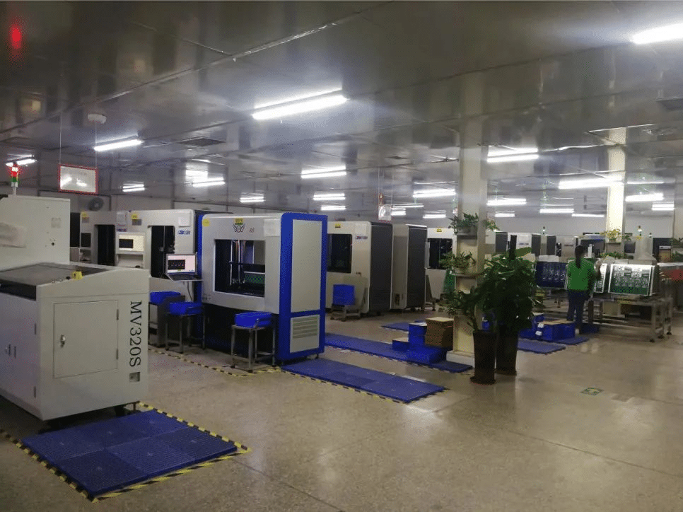
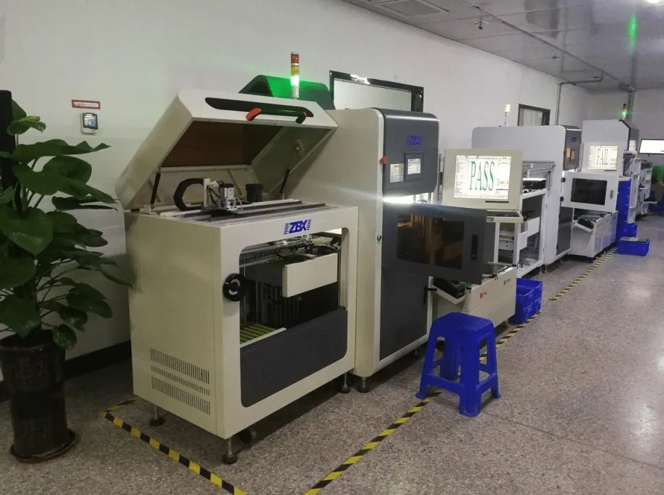
As shown in Figure 10-2, this is a flying probe tester actively testing boards.
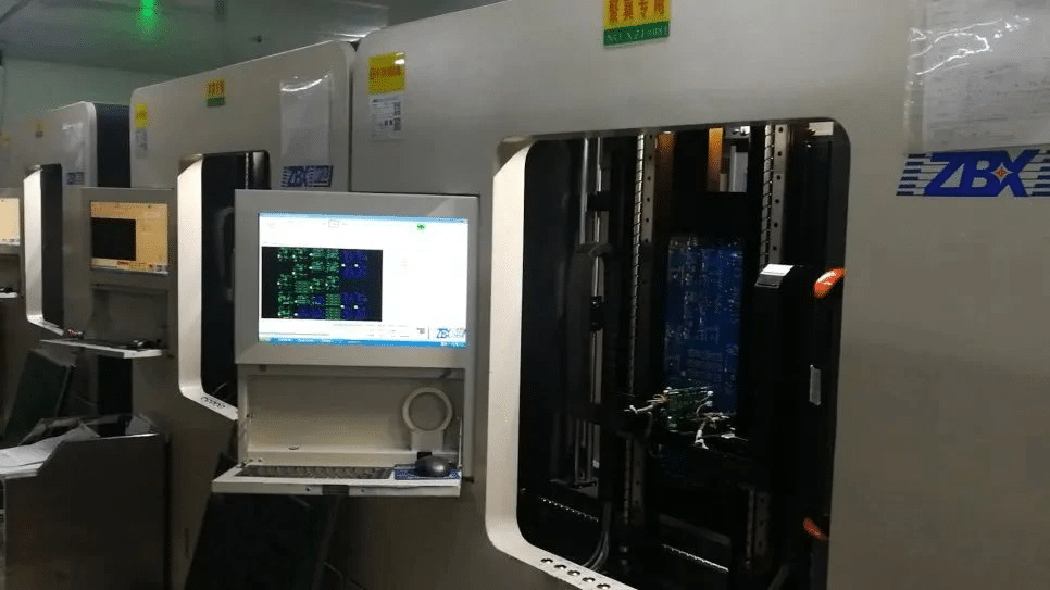
In Figure 10-3, we see two probe arms working in tandem. In fact, there are four probe arms operating simultaneously – two additional arms contact the back side of the board, not visible in the image.
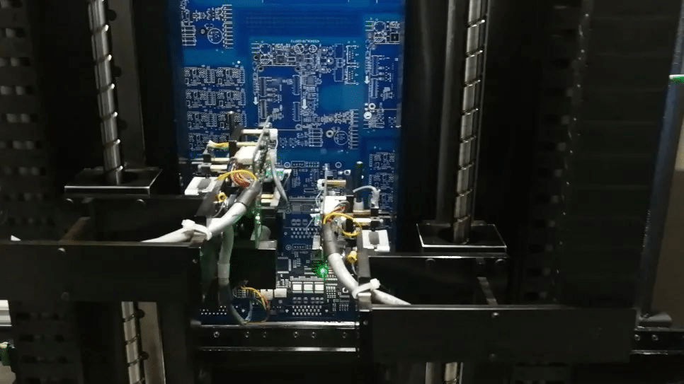
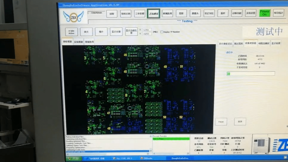
Figure 10-4 shows the computer display of a flying probe testing machine. The green pads indicate net points already tested, while blue pads show pending tests. Numbered regions are visible – the software divides the PCB into zones, preventing probe collisions during high-speed testing.
The probes move rapidly, stepping point-to-point to check each net. Despite this speed, with numerous points and traces per board, tests range from 20 minutes to 3 hours. Data shows the flying probe finding defects that continuity testing could miss, like corroded traces still conducting but out of spec. This rigorous validation ensures only the highest quality boards ship to customers.
Fixture Testing
As we learned, flying probe testing a single PCB is time-intensive. To address this, fixture-based testing was developed to validate boards in seconds.
Figure 10-5 shows the fixture testing equipment at JHYPCB. These testers use purpose-built jigs, custom-fitted to each board design. Operators quickly secure boards to the text fixture, then actuators press spring-loaded probes onto relevant testpoints. An analog circuit detects continuity between nodes, while integrated fixture circuitry simulates operation. Within moments, boards are electrically and functionally validated against the original schematics.
Fixture testers deliver blazing throughput – essential for high-volume production. However, their custom jigs are cost-prohibitive for low-volume runs. Our strategic hybrid approach combines the flexibility of flying probes with parallelized fixture verification, balancing quality, speed and affordability. This dual-testing workflow checks every detail while maintaining rapid turnaround, getting thoroughly validated boards to market faster.
While fixture testing is rapid, custom jigs must be fabricated – layered boards integrating probes, cabling, and test electronics. Constructing these fixtures incurs costs and lead times, so fixtures suit high-volume production. For prototypes, flying probes remain ideal.
Fixtures employ arrays of probes making simultaneous contact, testing entire boards in seconds – vastly faster than flying probes stepping point-by-point. However, this parallelism demands upfront fixture outlays, balancing speed with flexibility.
After electrical validation, PCBs proceed to routing and V-scoring – contour milling boards from panels and slicing routing lanes to facilitate depanelization. Testing verifies board functionality before this mechanical processing and shipment preparation.
Step 11: Routing and V-CUT
In all preceding steps, our circuit board has consistently existed in the form of a large panel. This step involves dividing the large panel into smaller boards, each representing a unique circuit board designed for a specific customer. Ultimately, these individual boards will be dispatched to different clients.
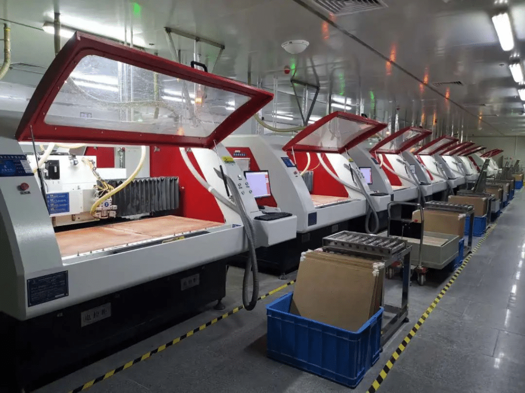
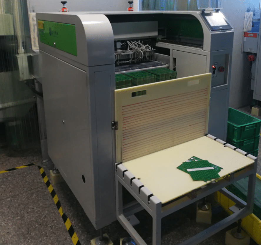
As illustrated in Figure 11-1, this corner of JHYPCB’s milling workshop showcases the routing machine used in the process.
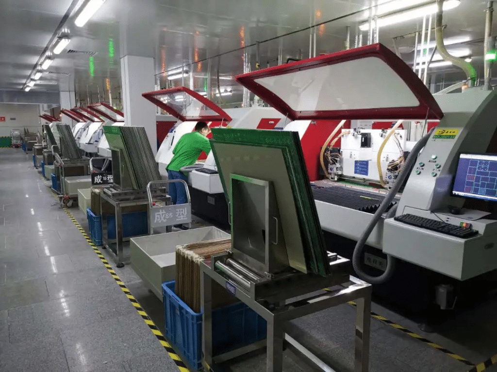
Routing, in this context, involves cutting the circuit boards from the larger panel according to the customer’s PCB outline design. If the board features irregular slots or special features like figure-eight holes, the process begins with milling internal slots before proceeding to the beveling step.
As depicted in Figure 11-2, a routing machine is milling internal slots for the circuit board.
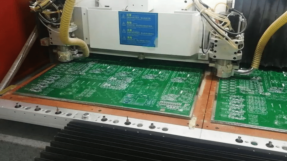
After the completion of milling internal slots or if there are no special slots, the process proceeds directly to the beveling step. Figure 11-3 illustrates that the routing machine is engaged in the routing process.
In the picture, we can see that there is an additional layer of paperboard on top of the circuit board, serving as protection. The beveling machine operates in a sequence of vertical and then horizontal cuts, completing all necessary vertical cuts in the large panel before proceeding to horizontal cuts.
The resulting circuit board after cutting is shown in Figure 11-4. As observed, there are numerous debris on the circuit board.
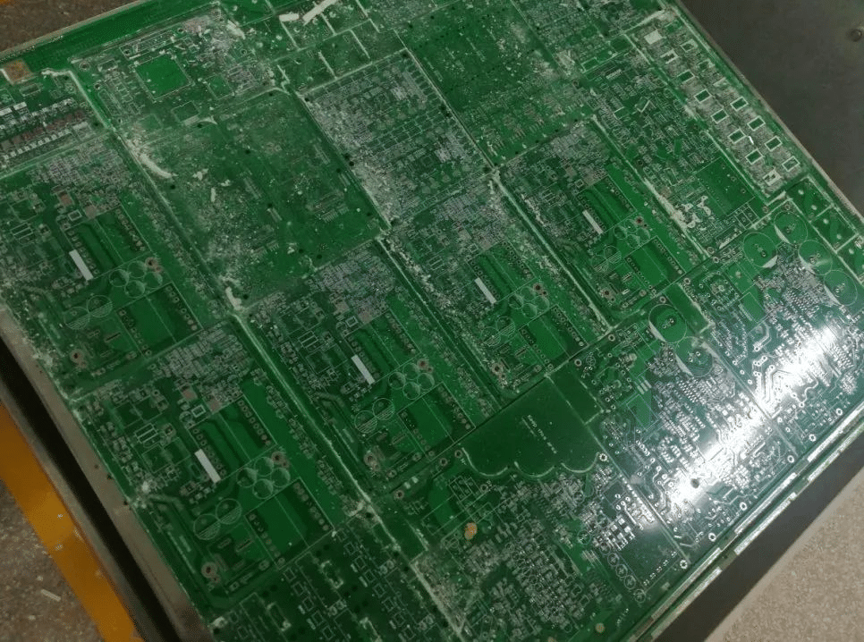
After the cutting process is complete, sorting can commence. During the sorting process, it’s essential to identify which boards require V-CUT, also known as V-grooving. Circuit boards that are assembled together, known as panelization, typically undergo V-grooving. The key distinction between V-grooving and beveling lies in the fact that beveling directly separates two circuit boards, whereas V-grooving leaves a portion uncut, requiring only a slight force to separate the two boards.
As depicted in Figure 11-5, JHYPCB employs a V-grooving machine in their process.
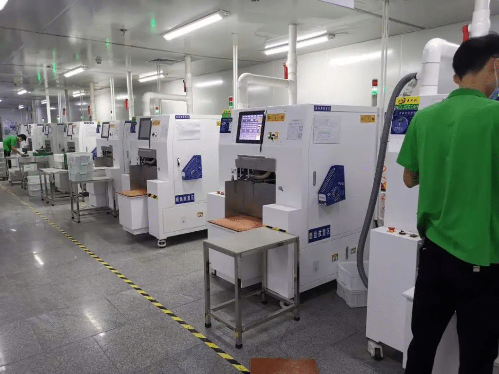
After the cutting process, we observed that there were many debris on the boards. Therefore, JHYPCB has an additional step of board washing. As shown in Figure 11-6, this is the initial board retrieval machine in JHYPCB’s board washing line.
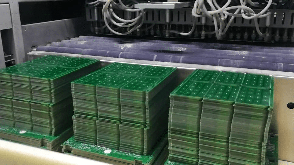
In Figure 11-7, circuit boards awaiting cleaning are arranged, and at the top, there is a suction plate device. This device moves above the circuit boards, suctioning three boards at a time and placing them on the roller line, guiding the circuit boards into the board washing line.
Once the circuit boards enter the production line, they undergo a sequence of processes, including acid washing, ultrasonic cleaning, pressure washing, rinsing with clean water, and drying. After completing these steps, the board washing process is finished. The cleaned boards are then sent to the Quality Control (QC) department.
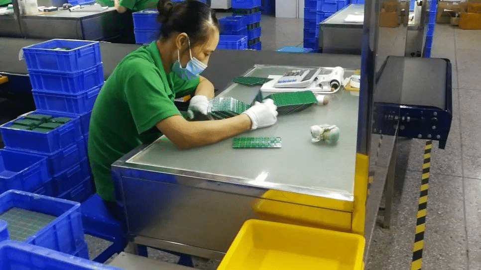
Step 12: Quality Control (QC)
QC, short for Quality Control, is the stage where manual inspection is primarily conducted. The focus is on assessing the appearance and quantity of the boards. Regarding the appearance, the inspection looks for noticeable defects such as scratches, blurred characters, and checks whether the boards requiring V-grooving have been appropriately processed.
As shown in Figure 12-1, this is a glimpse of JHYPCB’s QC workshop. Above the blue baskets, labels are affixed containing information such as customer numbers, internal identifiers, quantity, and more.
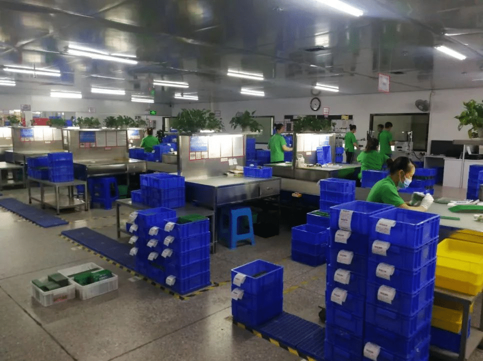
After the preceding processes of beveling, V-grooving, and board washing, the circuit boards are sent to the QC department. Upon arrival, they undergo a “beveling count” phase, primarily aimed at obtaining the label mentioned earlier.
We are aware that somewhere on the circuit board, there is our customer number. This is added to the circuit board by JHYPCB’s engineering team when creating the MI file. The personnel responsible for the beveling count, upon receiving the circuit board, locate the customer number and input it into the ERP system. Subsequently, they can print out the label.
After printing the barcode, it is affixed to the corresponding circuit board basket and handed over to the inspection personnel. Once the barcode is printed, we can track the progress of our circuit board in the JHYPCB Assistant, reaching the QC stage.
As shown in Figure 12-2, a JHYPCB inspector is checking the quantity.
After the QC process is complete, it is time for packaging and shipping.
Step 13: Shipping
Before shipping, packaging is conducted.
Upon receiving the circuit boards from QC, the first step is to print a packing label. This label contains essential information, and some customers, when placing orders with JHYPCB, may choose personalized parameters. For example, packaging preferences may include opting for JHYPCB branded boxes or plain unmarked boxes. After printing the label, the progress tracking in JHYPCB’s order assistant allows us to see that our circuit boards have entered the shipping stage.
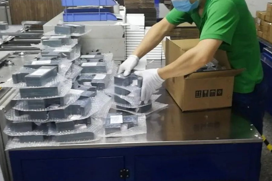
JHYPCB typically employs vacuum packaging. As depicted in Figure 13-1, this is JHYPCB’s vacuum packaging machine, with neatly arranged circuit boards awaiting packaging. Beside each stack of circuit boards, small bags of desiccant have been placed for moisture control.
If the customer’s order consists of a substantial quantity of boards, they are organized into multiple stacks. Each stack is labeled with information such as batch number, quantity per pack, and total quantity. Once the vacuum packaging is complete, the next step is boxing.
As shown in Figure 13-2, JHYPCB team members are in the process of boxing after the vacuum packaging. This is a small batch order. Before boxing, foam corner supports have been placed at the four corners of the box to prevent any potential damage to the circuit boards during transportation or handling.
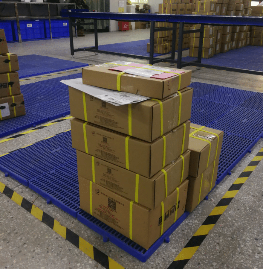
When there is a substantial number of boards, the boxes are typically larger. In such instances, the boxes undergo a “strapping” process for additional protection. As shown in Figure 13-3, this is a packaging box that has undergone the strapping process.
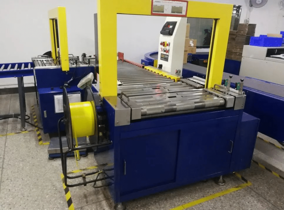
As shown in Figure 13-4, this is JHYPCB’s automated strapping machine.
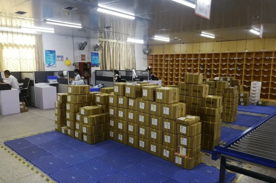
After the packaging is complete, the next step is the shipping process. Based on the information on the labels of the packaging boxes, the electronic waybill can be generated. As depicted in Figure 13-5, this is a corner of JHYPCB’s shipping department.
At this point, the manufacturing process of a double-layer PCB is complete. I hope this walkthrough has provided you with a better understanding of the PCB production process. Are you now more familiar with the PCB manufacturing process?


