Introduction: Definition, Role, and Types of Vias in PCBs
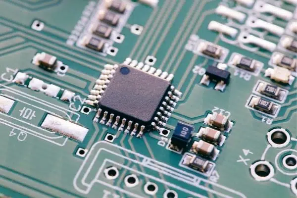
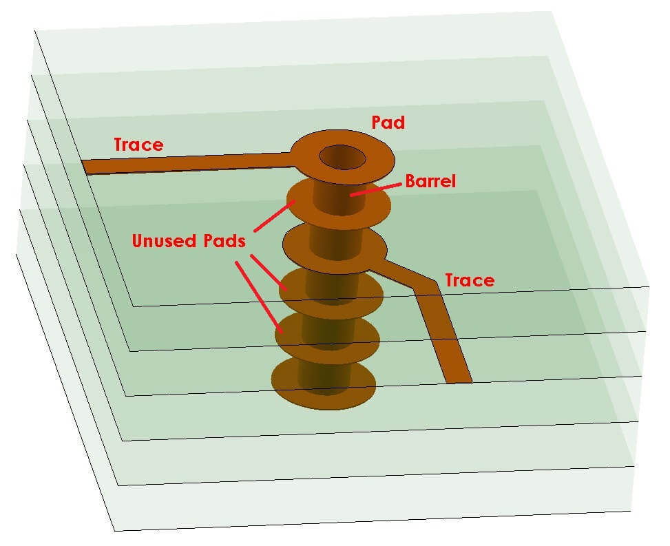
A via is a vertical electrical connection between layers in a printed circuit board. Vias enable traces to transition between layers to facilitate complex routing pathways and component connections within a confined PCB area or across multilayer PCB boards.
Vias play several important roles in PCBs. They provide vertical interconnections between copper layers, allowing signal traces and component leads to span between layers. Vias are also used strategically for shielding, heat transfer, grounding, and other functions. Additionally, component leads can be directly soldered into plated through-hole vias.
There are three major types of vias:
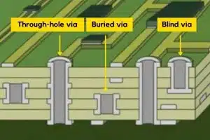
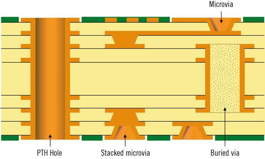
- Plated Through-hole Vias: Fully plated vias spanning the entire board vertically between layers. Plated through-hole vias (PTHs) enable robust layer transitions.
- Blind or Buried Vias: Partial-depth vias connecting internal layers without spanning fully through the board. Blind vias connect one internal layer to an external layer, while buried vias connect internal layers only.
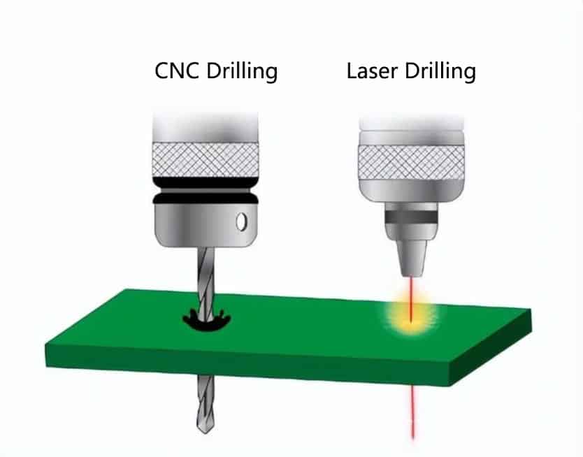
- Micro Vias: Small diameter vias, typically below 0.15mm, created with laser drilling. Micro vias facilitate connections in high density PCBs.
The rest of this article provides an in-depth overview of everything related to PCB vias, including their functions, construction methods, reliability factors, and innovative via technologies that enable advanced PCB performance and designs.
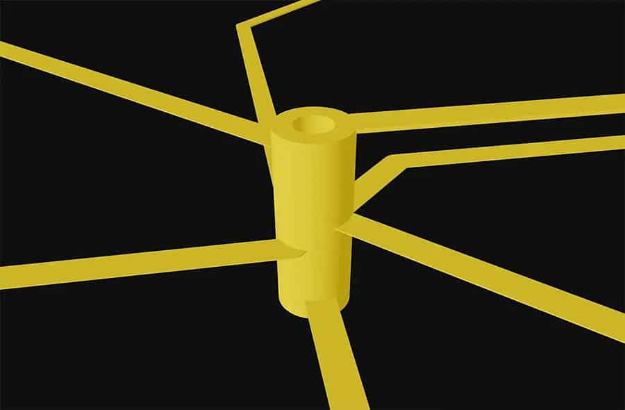
Table of Contents
Functions of Vias
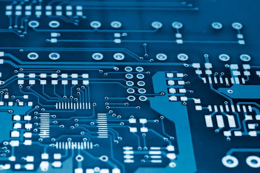
Vias serve several critical functions in PCBs:
- Interlayer Connections:
The primary function of vias is enabling vertical transitions of traces between layers. This allows routing traces on one layer to another destination layer to access pads, escape routing congestion, and so on. Strategic use of vias is essential for complex multilayer boards. - Component Connections:
Many through-hole component leads are soldered directly into plated through-hole vias. The via forms a robust mechanical attachment point while connecting traces between layers. - Grounding and Shielding:
Frequent vias help stitch ground planes between layers, lowering impedance for sensitive signals. Plated through-hole vias also allow soldering cable shields. - Heat Dissipation:
Vias provide thermal columns for heat sinking and cooling. Filled vias in particular enhance vertical heat conduction. - Signal Routing:
Microvias especially are integral for routing high-speed signals point-to-point between layers with minimal stub length, maintaining signal integrity.
In summary, innovatively leveraging vias enables routing density, signal performance, and overall functionality that would not be possible with a single layer PCB board. We next explore how vias are physically constructed to fulfill their wide-ranging design roles.
Via Construction and Materials
Creating a via is a complex, multi-step manufacturing process with precision and reliability considerations at each step. Here are key aspects of how vias are physically constructed:
- Drilling:
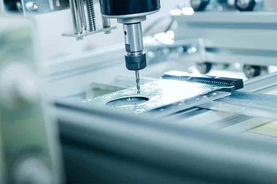
A mechanically drilled hole or laser drilled ablation forms the basic hole of the via. Drill precision impacts reliability. Lasers enable small microvias. - Plating and Filling:
The raw hole is plated with copper, facilitating soldering and conductivity between layers. Common platings include tin, silver, and occasionally gold over nickel. Filling non-conductive epoxy protects against contamination while boosting structural integrity. - Pad Design:
The pad shape and size must match drill tolerances while allowing sufficient solder volume. Common shapes include circular, rectangular, and rounded rectangular. - Anti-Pad:
The anti-pad is a clearance area isolating the via from adjacent copper to prevent shorting between layers during plating process overflows.
Additionally, more advanced fabrication processes have been developed, including carbon ink filling to replace plating and laser direct structuring (LDS) which selectively applies plating.
In the next sections we analyze the reliability impacts of precision manufacturing and discuss cutting-edge innovations enabling the highest via performance to match increasing PCB demands.
Via Reliability Considerations
While vias enable advanced PCB functionality, they can also be sources of failure without proper design and fabrication. Understanding common failure modes and managing risk factors is key to ensuring via reliability.
- Failure Modes:
Typical via failures include cracked barrels, lifted pads, incomplete plating, and loose solder joints. Reliability testing methods include thermal cycling, vibration, mechanical shock, and electrical testing. - Reliability Factors:
Drilling accuracy and plating thickness directly impact reliability. Tighter tolerances reduce vibration failures but increase cost. Thermal expansion also strains vias over temperature cycling. - Reliability vs. Density Tradeoffs:
Smaller microvias are more prone to failure but allow greater routing density. Shielding, adequate anti-pad clearances, and limitation of aspect ratios can optimize reliability, balancing performance and yield.
In conclusion, while innovating new via capabilities, it remains critical to validate designs through modeling, testing, and ultimately years of field reliability data. Vias are a fundamental building block of advanced, reliable PCBs when engineered appropriately for the application.
Next we discuss advanced via structures pushing the boundaries of what’s possible while maintaining reliability.
Advanced Via Structures and Techniques
As PCBs become denser and more complex, new innovations in via fabrication allow enhanced capabilities. Here are some advanced via types and technologies:
- Backdrilled Vias:
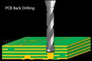
The via barrel extends through the pad on outer layers, then is mechanically drilled off to remove the stub section. This significantly reduces stub resonance for high-speed signals. - Filled & Capped Vias:
Completely filling a via’s hole eliminates contamination risks and boosts heat transfer compared to only plated vias. Capped vias cover just the end holes with protective epoxy. - Tented Vias:
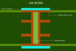
A layer of solder mask coating isolates tented vias entirely, preventing solder and debris from entering vias not used for component terminals. - Via in Pad (VIP):
VIP places drill pads over function pad centers, allowing vias embedded directly within footprints that would otherwise block routing channels. - Laser Assisted Microvias:
Lasers drill small diameter holes not possible with mechanical bits, then facilitate direct copper plating with no seeding required.
In conclusion, as PCBs continue advancing into 5G wireless, automotive, and other cutting-edge applications, innovating robust via implementation and reliability will remain critical for ongoing performance increases.
Conclusion
Vias enable the sophisticated functionality of modern PCBs by allowing vertical transitions of electrical connectivity across multiple routing layers. As discussed in this article, they serve diverse roles from facilitating dense component placement to shielding sensitive signals and conducting heat.
A wide array of via types have been developed, from basic plated through-holes to microvias under 0.15mm diameter. Reliability considerations around material selection, drilling precision, and testing are critical to avoid failure modes like cracks or lifted pads. Tradeoffs exist between high-density layouts and production yields.
Ongoing innovations around backdrilling, filling methods, and laser materials processing allow PCB designers to keep pushing the envelope. 5G telecom and automotive electronics especially drive via performance requirements. However, new via capabilities must balance density with validating designs through prototyping and field reliability over thousands of thermal cycles.
With sound engineering practices, vias enable the cutting-edge PCBs underlying everything from smartphones to flight systems by allowing ever-greater layout densities and electrical performance envelope-pushing. As PCB trends like high-frequency signals, embedded passives, and thinner substrates advance, expect vias to continue playing a fundamental yet evolving role.

