In the soldering process (SMT: Surface Mount Technology and THT: Through-hole Technology) of the PCB assembly industry, more and more SMT manufacturers have begun to turn their attention to selective wave soldering (selective soldering). Selective Soldering can complete all solder joints at the same time, minimizing production costs; at the same time, it overcomes the problem of reflow soldering affecting temperature-sensitive components, and selective soldering is also compatible with lead-free soldering, these advantages make the application range of selective soldering more and more extensive.
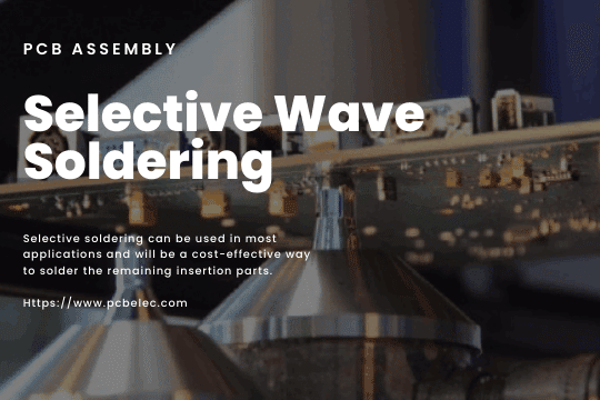
Looking back on the development process of the electronics industry in recent years, we can see that a clear trend is reflow soldering technology. In principle, traditional insertion parts (through-hole device) can also be used in a reflow soldering process, commonly referred to as through-hole reflow soldering technology. The advantage is that it is possible to complete all solder joints simultaneously, keeping production costs to a minimum. However, temperature-sensitive components have limited the application of reflow soldering, whether it is insertion parts or SMD (Surface Mount Device), and people have turned to selective soldering. Selective soldering after reflow soldering can be used in most applications and will be a cost-effective way to solder the remaining insertion parts.
The Rise and Development of Selective Wave Soldering
With the rapid development of modern electronic information technology, integrated circuit chip packaging forms are emerging one after another, and the packaging density is getting higher and higher, which significantly promotes the development of electronic products in the direction of multi-function, high performance, high reliability, and low cost. However, the components have not been entirely chip-typed. Due to the low-cost advantage of through-hole assembly, through-hole components are still widely used on many occasions. As electronic assemblies become denser, some through-hole assemblies cannot be soldered with traditional wave soldering. Selective wave soldering is a unique form of wave soldering technology developed to meet through-hole component soldering development requirements to achieve the best welding quality. It is generally composed of flux spraying, preheating, and welding. Through the equipment programming device, the flux spraying module can complete the selective flux spraying for each solder joint in turn. After the preheating module is preheated, the soldering completes welding point by point for each solder joint. Selective wave soldering is a newly introduced process. It is necessary to conduct process research on selective wave soldering and find suitable parameters to reduce production costs and improve welding quality.
The history of modern electronic welding technology has undergone two historical changes: the first is from through-hole welding technology to the transformation of surface mount welding technology; the second is from lead welding technology to the transformation of lead-free welding technology. The evolution of soldering technology has directly brought about two results: firstly, fewer and fewer through-hole components need to be soldered on circuit boards; secondly, through-hole components (especially large thermal capacity or fine-pitch components) are becoming more and more difficult to solder, especially for products with lead-free and high-reliability requirements. Then there are the new challenges facing the global electronics assembly industry: global competition is forcing manufacturers to bring products to market in less time to meet changing customer requirements; seasonal changes in product demand require flexible manufacturing concepts; global competition is forcing manufacturers to reduce operating costs while improving quality, and lead-free production has become a major trend. All of the above challenges are naturally reflected in the choice of production methods and equipment, which is the main reason why selective wave soldering has developed faster than any other soldering method in recent years; of course, the advent of the lead-free era is another critical factor driving its development.
Through-hole components are soldered using several soldering techniques such as manual soldering, wave soldering and selective soldering, which have different characteristics.
This article introduces the knowledge of PCB selective soldering technology and process, including the definition of PCB selective soldering technology, characteristics, the difference between selective soldering and wave soldering, the process flow of selective soldering technology, and the two different processes of selective soldering: drag soldering process and dip soldering process.
Process characteristics of selective soldering of circuit boards
Selective soldering is one of the processes used to manufacture various electronic assemblies(usually circuit boards). Typically, the process involves soldering specific electronic components to a printed circuit board without affecting other areas of the board. In practice, selective soldering can refer to any soldering method, from manual soldering to specialized soldering equipment, as long as the method is precise enough to use solder only in the desired area.
The difference between selective soldering and wave soldering
Its difference from wave soldering can understand the process characteristics of selective soldering of circuit boards. The most apparent difference between the two is that the lower part of the PCB is completely immersed in the liquid solder in wave soldering. In selective soldering, only some specific areas are in contact with the solder wave. Since the PCB itself is a poor heat transfer medium, it does not heat and melt the solder joints in adjacent components and PCB areas when soldering. Compared with wave soldering, the flux is only applied to the lower part of the PCB to be soldered, not the entire PCB. In addition, selective soldering is only suitable for soldering insertion components. Selective soldering is an entirely new method of soldering, and a thorough understanding of the selective soldering process and equipment is necessary for successful soldering.
Further reading
1. What is selective wave soldering?
Selective wave soldering, also known as selective soldering, is used in the field of through-hole soldering of PCB insertion parts. Due to its different welding advantages, selective wave soldering has gradually become popular and is widely used in the welding of through-hole parts of multi-layer PCBs with high welding requirements and complex processes, such as military electronics, spacecraft electronics, automotive electronics, digital cameras, and printers.
There are two types of selective wave soldering: offline selective wave soldering and online selective wave soldering.
Off-line selective wave soldering: Off-line refers to the method offline from the production line. The solder resist spraying machine and the selective soldering machine are split 1+1, in which the preheating module follows the welding part, manual transmission, and human-machine combination. The device takes up less space.
Online selective wave soldering: The online system can receive production line data in real-time and automatically connect. Solder resist module, preheating module, welding module integrated structure, characterized by automatic chain transmission. However, the equipment occupies ample space and is suitable for production modes with high automation requirements.
Offline and online PCB selective wave soldering machine
2. Manual welding
Manual welding is still widely used today due to its long history, low cost, and high flexibility. However, in some applications with high-reliability requirements and difficult welding, they are pretty restricted due to the following reasons:
1) The temperature of the soldering iron tip is difficult to precisely control, which is the most fundamental problem. If the temperature of the soldering iron tip is too low, it is easy to cause the soldering temperature to be lower than the lower limit of the process to form cold soldering or virtual soldering; at the same time, it is also very easy to cause poor tin penetration in the metallized through holes. If the temperature of the soldering iron tip is too high, it is easy to make the soldering temperature higher than the upper limit of the process to form an excessively thick intermetallic compound layer, which will cause the solder joint to become brittle and the strength will decrease, and may cause the pad to fall off and the circuit board to be scrapped.
2) The quality of solder joints is often affected by the operator’s knowledge, skills, and emotions, and it is difficult to control.
3) The cost advantage of labor over machinery and equipment is gradually being lost.
The process of selective soldering on circuit boards
Typical selective soldering processes include flux spraying, circuit board preheating, dip soldering, and drag soldering.
1. Flux coating process
In selective soldering, the flux coating process plays an important role. The flux should be active enough to prevent bridging and prevent oxidation of the PCB during solder heating and at the end of soldering. The x/y manipulator carries the flux spraying to pass the PCB over the flux nozzle, and the flux is sprayed onto the PCB to be soldered. Flux has a single nozzle spray, micro-hole spray, synchronous multi-point / pattern spray. The most important thing for selective wave soldering after the reflow process is the accurate spraying of the flux. Microbore jet will never stain areas other than solder joints. The minimum flux point pattern diameter of micro-spray spraying is greater than 2mm, so the position accuracy of the flux deposited on the PCB is ±0.5mm to ensure that the flux always covers the welded part. Tolerances for the amount of flux sprayed are provided by the supplier. The technical specification should specify the amount of flux to be used; usually, a 100% safety tolerance range is recommended.
2. Preheating process
The primary purpose of preheating in a selective soldering process is not to reduce thermal stress but to pre-dry the flux to remove the solvent so that the flux has the correct viscosity before entering the solder wave. During soldering, the influence of the heat brought by preheating on the soldering quality is not a key factor. The thickness of the PCB material, device package specifications, and flux type determine the preheating temperature setting. There are different theoretical explanations for preheating in selective soldering: some process engineers believe that the PCB should be preheated before fluxing; another view is that preheating is not required and soldering is performed directly. The user can arrange the process flow of selective welding according to the specific situation.
3. Types of Selective Soldering Processes for Circuit Boards
There are two different processes for selective soldering: drag soldering and dip soldering.
How selective wave soldering works
The selective drag soldering process is done on a single small tip solder wave. The drag soldering process is suitable for soldering in very tight spaces on the PCB board.
For example, individual solder joints or pins and single row pins can be subject to the drag welding process. The PCB moves on the solder wave of the solder tip at different speeds and angles to achieve the best solder quality. To ensure the stability of the welding process, the inner diameter of the welding tip is less than 6mm. After the flow direction of the solder solution is determined, the nozzles are installed and optimized in different directions for different soldering needs. The manipulator can approach the solder wave from different directions, that is, different angles between 0° and 12°, so that the user can solder various devices on the electronic components. For most devices, the recommended tilt angle is 10°.
Compared with the DIP welding process, the solder solution of the drag welding process and the movement of the PCB board make the heat conversion efficiency better than the DIP welding process. However, the solder wave transfers the heat required to form the weld connection, and the solder wave of a single nozzle is small. Only the temperature of the solder wave is relatively high can it meet the requirements of the drag welding process.
Example: Soldering temperature of 275℃~300℃ and drag speed of 10mm/s~25mm/s are usually acceptable. Nitrogen is supplied in the welding area to prevent the oxidation of the solder wave. The solder wave eliminates the oxidation so that the drag welding process avoids the generation of bridging defects. This advantage increases the stability and reliability of the drag welding process.
The machine has the characteristics of high precision and high flexibility. The modular structural design can be customized entirely according to the unique production requirements of customers and can be upgraded to meet the needs of future product development. The movement radius of the robot can cover the flux nozzle, preheat, and solder nozzle so that the same equipment can complete different welding processes. The machine-specific synchronous process can significantly shorten the single-board process cycle. The capabilities of the manipulator give this selective welding the characteristics of high-precision and high-quality welding. The first is the highly stable and precise positioning capability of the manipulator (±0.05mm), which ensures that the parameters produced by each board are highly repeatable and consistent; the second is the 5-dimensional movement of the manipulator, which enables the PCB to contact the tin surface at any optimized angle and orientation to obtain Best welding quality. The tin wave height stylus installed on the manipulator splint device is titanium alloy. Under the program control, the tin wave height can be measured regularly, and the tin wave height can be controlled by adjusting the speed of the tin pump to ensure process stability.
Despite all the advantages mentioned above, the single-nozzle solder wave drag soldering process also has shortcomings: the soldering time is the longest among the three processes of flux spraying, preheating, and soldering. And because the solder joints are drag soldered one by one, as the number of solder joints increases, the soldering time will increase significantly, which cannot be compared with the traditional wave soldering process in terms of soldering efficiency. But things are changing, and multi-tip designs can maximize throughput; for example, using dual solder nozzles can double the output, which also can be done for flux.
Dip selective soldering systems have multiple solder nozzles and are designed one-to-one with the points soldered on the PCB. Although the flexibility is not as good as that of the manipulator, the output is equivalent to traditional wave soldering equipment. The equipment cost is lower than that of the manipulator. Depending on the size of the PCB, single-board or multi-board parallel transfer can be performed, and all joints to be soldered will be fluxed, preheated, and soldered at the same time in parallel. However, special solder nozzles need to be made for different PCBs due to the different distribution of solder joints on different PCBs. The size of the solder tip is as large as possible to ensure the stability of the soldering process without affecting the adjacent peripheral devices on the PCB, which is essential and difficult for the design engineer because the stability of the process may depend on it.
The solder joints of 0.7mm to 10mm can be soldered using the dip selective soldering process. The soldering process of short pins and small-sized pads is more stable, and the possibility of bridging is slight. The distance between the edges of adjacent solder joints, devices, and soldering tips should be greater than 5mm.
Precautions for carrier and circuit design layout of selective wave soldering
- When the solder pins of traditional through-hole components are too close to the edge of the carrier, it is easy to cause solder insufficiency due to the shadow effect.
- The carrier must cover the parts that do not need to be soldered in a solder pot.
- Keeping at least 0.05″ (1.27mm) of wall thickness at the edge of the hole in the carrier is recommended to ensure isolation of solder penetration into those parts that do not need to be soldered in a solder pot.
- It is recommended to keep at least 0.1″ (2.54mm) from the edge of the hole in the carrier for parts that need to be soldered in a tin furnace to reduce the possible shadow effect.
- The material of the carrier should not react with the solder and should be able to withstand repeated high-heat cycles without deformation, not easy to absorb heat, and should be as light as possible with less thermal shrinkage. Many people use aluminum alloy material, and some use synthetic stone material.
Advantages of selective wave soldering
- No unique fixtures and trays are required for welding.
- Through-hole parts do not require reflow-resistant materials
- Good soldering quality and through-hole filling rate can be obtained during soldering.
- Save energy. Selective soldering does not require a solder pot as large as wave soldering nor a heating zone as long as a reflow oven to achieve its purpose.
- Cost savings. Selective soldering does not require many solder bars like wave soldering.
- The circuit board is not easy to bend and deform due to high temperature
- Selective soldering saves time compared to traditional wave soldering and SMT
- For solder joints with different welding difficulties, the welding time can be set in a targeted manner to ensure the welding quality.
Disadvantages of selective wave soldering
- Additional equipment must be purchased for selective wave soldering
- Compared with SMT, selective wave soldering must reserve a relatively large avoidance area.
Note: The avoidance area, also known as the clearance area, generally refers to where parts cannot be placed. There should be at least a particular “relief zone” between the through-hole pins and the parts next to them to prevent short-circuiting with the through-hole pins or being hit by the selective soldering nozzle during selective soldering.
3. Selective wave soldering requires programming, so it is also a waste of pre-processing time, but it can be reused after programming.
4. The efficiency of selective wave soldering is low, especially the printed circuit board with more insertion parts is not suitable for this equipment.
In fact, when the circuit board first came out, it was almost always designed by traditional insertion operations, and all the boards also needed to go through wave soldering, and the boards at that time only had a single-sided PCB.
Later, after the invention of SMT technology, the mixed-use of SMT and wave soldering began to appear. Because at that time, there were still a large number of parts that could not be converted to the SMT process, which means that there were still many traditional through-hole parts. Therefore, when designing the board, all through-hole parts must be installed on the same side, and then use the other side for wave soldering, and the SMT parts on the wave soldering side must be fixed with red glue to prevent the parts falling in the furnace. Almost all boards have adopted the SMT process on both sides, but there are still very few parts that cannot be replaced by the SMT process, so this selective wave soldering process comes into being.
JHYPCB is a Shenzhen PCB circuit board manufacturer specializing in PCB prototype fabrication and assembly services. We have accumulated rich experience in quick turn PCB, PCB assembly, low volume to mass PCB production. We welcome customers to inquire and place orders.
Related Reading
- PCB Assembly Capability
- Turnkey PCB Assembly Service
- LED PCB Assembly
- Fast Prototype PCB Assembly Service
- Low Volume And Quick Turn PCB PCB Prototype Assembly Services
- Components Purchasing Services
- What is the Bill of Materials(BOM), and how to create one?
- Solder Paste and Solder Paste Printing in SMT PCB Assembly
- What is the difference between wave soldering and reflow soldering?
- SELECTIVE VS WAVE SOLDERING VS REFLOW SOLDERING: What Is The Difference?


