In the previous article, we covered the first and second steps of the PCB manufacturing process – MI (Manufacturing Instruction), which involves crafting a manufacturing instruction document tailored to the specifics of the customer’s PCB files, and drilling. This manufacturing instruction document serves as the guiding beacon for subsequent manufacturing processes. Drilling then punctures holes in the PCB according to the design to allow different layers to connect.
Now we build upon that foundation. Copper plating chemically deposits a thin layer of copper over the entire PCB surface, including the walls of the recently drilled holes. This forms the conductive traces that carry electricity. Routing then selectively removes excess copper to leave only the desired circuit pattern.
Step 3: Plated Through Hole
Fresh from the drilling process, the board is now dotted with holes. However, these voids are non-conductive as the walls are devoid of copper. The next critical step—copper plating, also called electroless plating, plated through hole (PTH), panel plating—deposits a thin conductive film, preparing the way for subsequent electroplating operations where copper and tin implant the tracings.
In a nutshell, copper plating fulfills two key functions:
- Coats all surfaces, including freshly minted hole walls, with a slim layer of conductive material
- Primes the board for graphical electrodeposition processes to embed circuitry
The copper plating production track is alternatively called the “conductive adhesive route.”
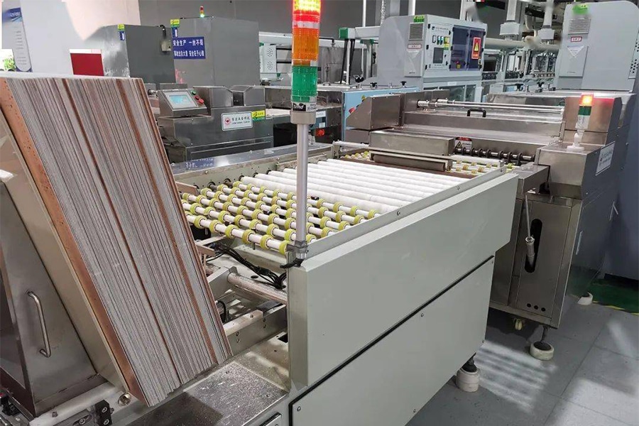
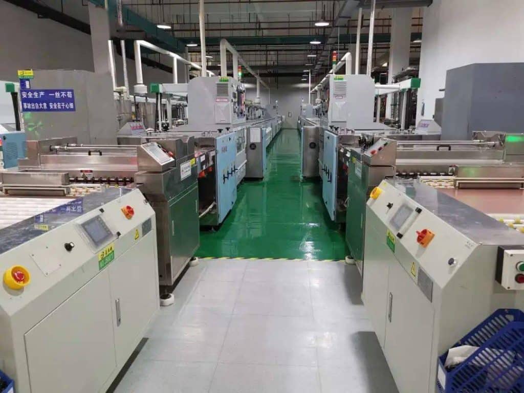
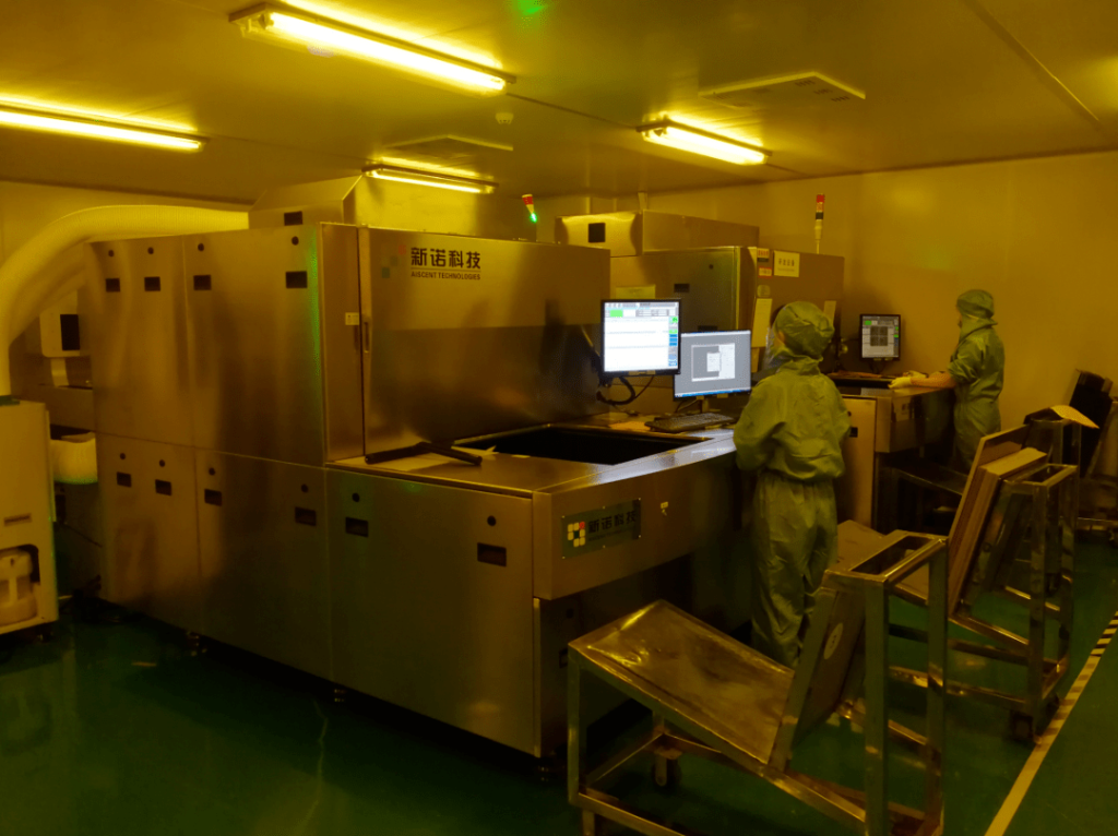
As depicted in Figure 3-1, JHYPCB operates two fully automated PTH lines. The overview shot spotlights the integrality of the process. As boards wend through the sequence, copper plating is consummated in a mere matter of minutes.
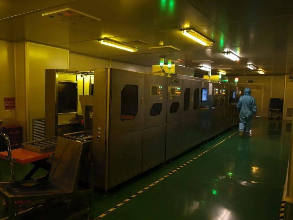
As shown in Figure 3-2, these are the boards that just came from the drilling process, covered in holes. We can see that the boards are waiting to enter the plated through hole line for copper plating.
The image shows the drilled boards before they undergo copper electroless plating. The boards are full of holes all over, queued up to enter the automated plated copper line where a thin coating of conductive copper will be deposited over the entire board surface, including the interior hole walls.
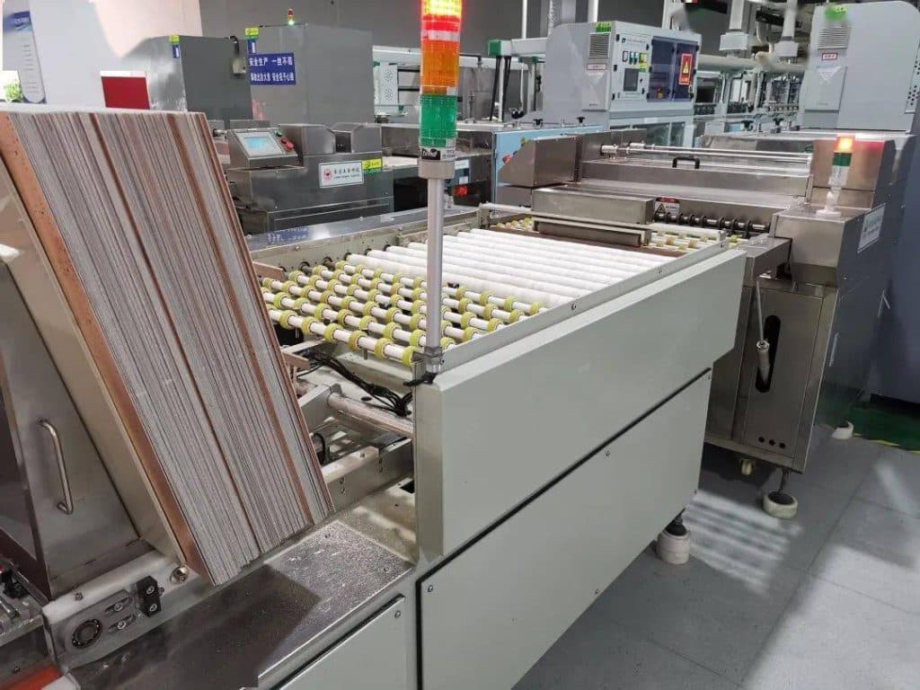
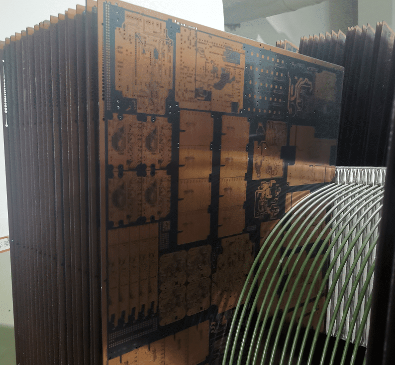
As depicted in Figure 3-3, drilled copper clad laminate boards have been positioned at the fore of the copper plating line. Upon activation, the conductive adhesive route sequentially feeds each panel into the production track.
Once online, the automated conductive glue sequence intakes drilled copper foil boards placed at the front end of the process. One by one, panels progress into the electroless plating workflow.
Upon entering the conductive glue line, boards first pass through a deburring machine as shown in Figure 3-4. After drilling, the copper clad laminate panels inevitably contain burrs and rough edges around the perforations. The deburring machine serves to smooth and flatten board surfaces.
Introducing the electroless copper plating sequence, initial stages involve a deburring stop. There, a grinding apparatus refines drilled foil boards – conditioning areas bordering holes and removing errant slivers. The process planes panels, securing an even finish before subsequent handling.
After deburring, the remaining process chain consists of chemical reactions. The key stages involve micro-etching, desmear, oxidation, polymerization, drying, and intermittent rinses.
Micro-etching cleans the surface oxide layer, removes grime, and creates micro-roughness to improve adhesion.
Desmear cleans hole walls, penetrates perforations, and enhances conductivity.
Oxidation uses an oxidizer to react with glass fiber resin on the hole walls, generating a chemical film.
Polymerization deposits a polymer coating on the hole walls to impart conductivity.
Drying first absorbs surface moisture with hydrophilic foam then blow dries remaining liquid with heated air.
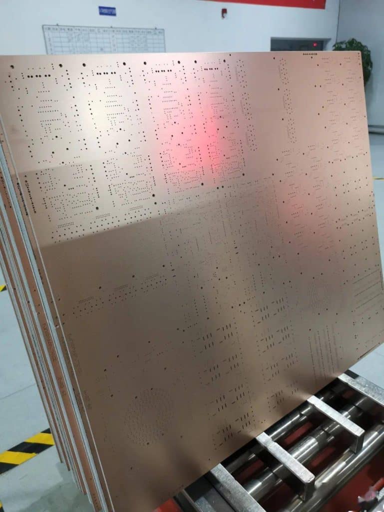
Post-copper plating, boards appear similar to their post-drilling state, albeit now with a conductive inner layer lining holes.
Freshly plated panels bypass directly to the next process: routing.
Step 4: Routing
The routing process consists of three key steps in sequence: lamination, exposure, and development. Upon completion, the copper clad laminate will exhibit clearly defined circuitry.
Lamination
In PCB fabrication, the terms “dry film” and “wet film” refer to this lamination process.
Compared to wet lamination, dry film delivers higher consistency and quality. JHYPCB utilizes the dry process.
Lamination applies an azure photosensitive film on both sides of the copper clad laminate.
Freshly plated boards transport directly from the production line to the routing room. There, the conveyor equips the panels with laminate in around one minute.
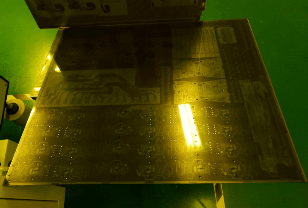
Post-lamination boards appear as shown in Figure 4-1. The blue film coating is visible, tinted yellow under the room’s lighting.
The photosensitive film enables circuitry imprinting onto the copper clad laminate. Its residence proves temporary, soon dissolving after fulfilling its purpose in subsequent pattern plating processes. Like a phantom, the laminate’s ephemeral embrace persists barely long enough to dispatch its imprint before evanescing from whence it came.
Serving as a transient template, the azure laminate catalyzes tracings through imagery transference. Upon conclusion of the electrodeposition step, these helpers have no further utility, their imprints permanently etched into copper canvases.
Exposure
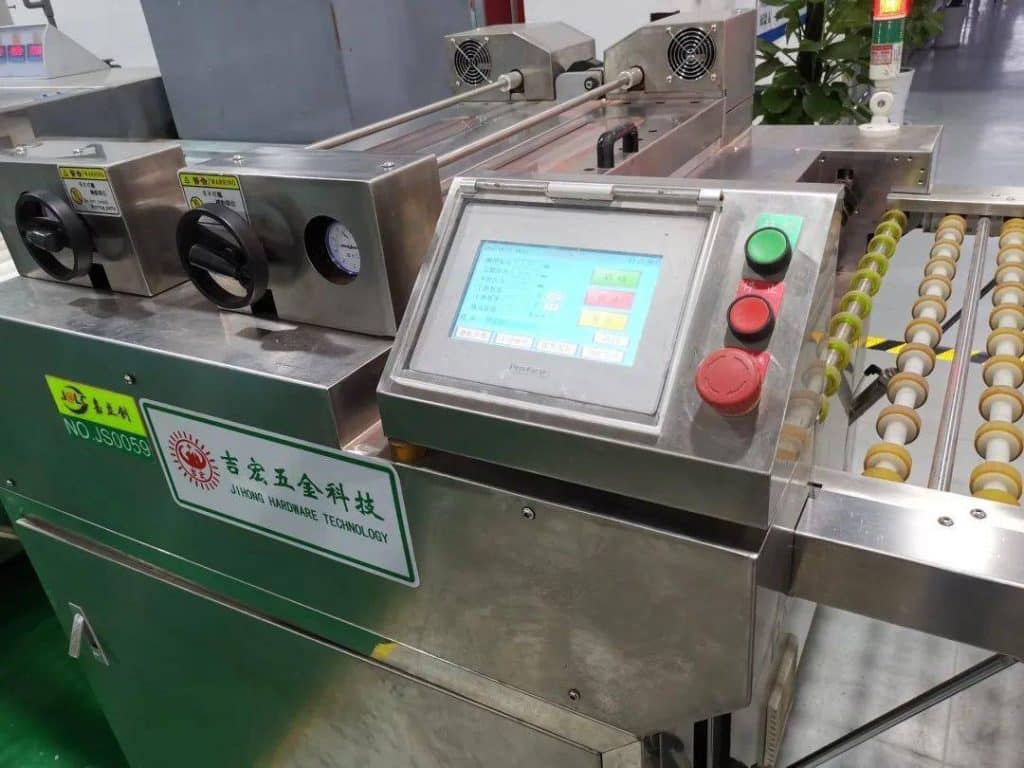
JHYPCB currently utilizes two exposure systems: a film-based automated machine and an LDI fully automated direct imager.
Figure 4-2 illustrates the former – An automatic exposure machine that requires film.
This automated exposure system requires film alignment with the laminated circuit boards prior to activation. The routing film transparencies exhibit opaque black tracings against a clear background. Under exposure lamps, unmasked areas receive complete light penetration to activate photosensitive laminate.
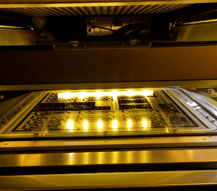
As illustrated in Figure 4-3, dark, intricate artwork imprinted on film negatives will soon transpose to copper substrates through selective illumination. Regions eclipsed by filament shadows emerge unexposed, future conduits spared from erosion.
The process transfers circuit layouts by casting a photomask template then selectively exposing surrounding spaces. This precipitates a pattern, to be shortly revealed, of conductive pathways amidst scooped trenches.
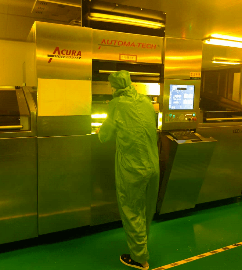
As shown in Figure 4-4, the LDI exposure system utilizes laser direct imaging technology, eliminating the need for film. It images circuit patterns directly onto dry film by extracting manufacturing instruction data. While convenient, LDI machines trail film-based automated exposure in speed. Therefore, LDI better suits prototyping applications, while high-volume production remains the domain of film-based processes.
The LDI direct laser exposure equipment depicted forgos physical negatives in favor of rastering artwork directly from digital manufacturing records. This expedites low-volume runs by omitting film development. However, pagination through gerber files indelibly limits cadence compared to lamp-shined transparencies. As such, LDI thrives serving prototype designs, whereas film-based processes accommodate high-mix production.
As depicted in Figure 4-5, an LDI-based automated production line for double-sided circuitry. As most boards require routing on both faces, the process necessitates exposing either side. While the system in Figure 4-4 relies on manual board flipping, Figure 4-5 shows conveyors equipped with automated inverters to streamline processing.
Whereas single-face etching suffices for elementary designs, multilayer boards commonly demand circuitry fore and aft. Exposing such symmetries once mandated manual palette rotation after initial imprinting, an inefficient bottleneck. Hence automated turret flip stations now feature, as exemplified in Figure 4-5. Panel turners inline with laser imagers upgrade throughput for dense double-sided constructions.
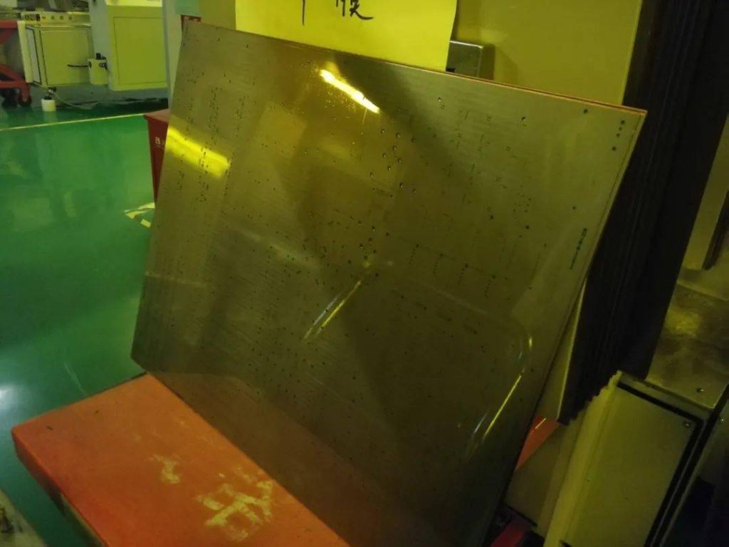
Post-exposure, distinct circuitry imprints become visible on the dry film as shown in Figure 4-6.
Subsequent to light infiltration, intricate tracings emerge on laminate, routes once shaded now bared. The selective illumination births shadows, limned paths ready to transplant. Latent images surface, ephemeral guides soon to give way as artwork etched in copper.
Development
Exposure enables subsequent development steps. Developer solution removes unexposed dry film, stripping away masked circuit regions to reveal copper beneath. Figure 4-7 displays a panel post-development.
The routing process concludes here. Next up: pattern plating!
In our forthcoming installment, we will explore the fifth and sixth stages – plating circuitry through graphical electrodeposition followed by automated optical inspection.


