Welcome to the intricate world of PCB manufacturing, where precision meets innovation. In this installment, we unravel the first steps of the process – Manufacturing Instruction (MI), Cutting, and Drilling. At JHYPCB, these foundational elements set the stage for the seamless creation of printed circuit boards. Let’s dive into the essential aspects of MI, material cutting, and drilling, understanding their significance in crafting top-notch PCBs.
Step 1: Manufacturing Instruction (MI)
Once a customer initiates a PCB order with JHYPCB by submitting PCB or Gerber files, our adept MI team takes the helm, meticulously crafting a manufacturing instruction document tailored to the specifics of the customer’s PCB files. This document serves as the guiding beacon for subsequent manufacturing processes.
Remarkably, the MI document isn’t confined to an isolated customer’s individual PCB board. Instead, it often amalgamates diverse PCB files from multiple customers into a slightly larger circuit board. Subsequently, a unified MI file is fashioned for this composite board, with details regarding its dimensions to be elucidated in the forthcoming Step 2, “Drilling.”
The MI file emerges as the linchpin in PCB production. Every subsequent manufacturing stride adheres to the directives encapsulated within this document. Executed with precision, the MI file is meticulously curated by the adept engineering department at JHYPCB’s Shenzhen headquarters.
Step 2: Drilling
Drilling initiates the formal PCB production process. The primary objective of drilling is to create perforations across the entire PCB board where holes are needed, encompassing electrical holes, mechanical holes, and through holes. (Irregular mechanical slot holes are not addressed in this step but are finalized in Step 11, referred to as “Routing.”)
The intricate steps involved in the drilling process, sequentially, are Material cutting, Pinning, and Drilling. Each of these steps is elucidated below.
Material Cutting
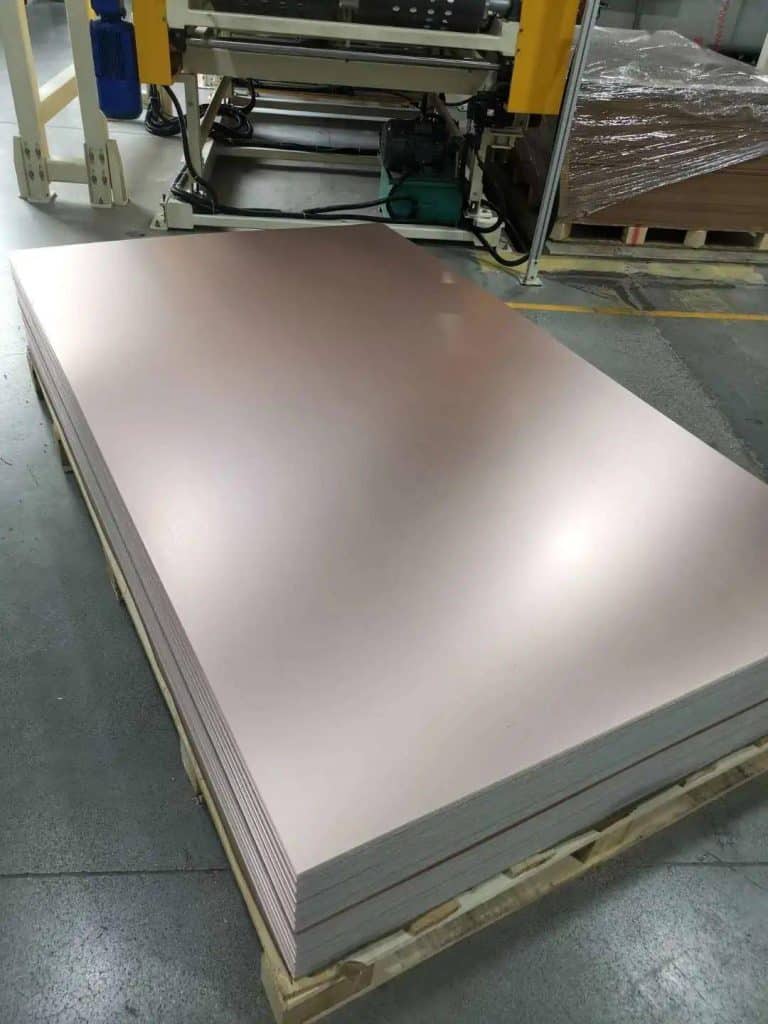
Before production begins, the PCB raw material is a copper clad laminate as shown in Figure 1. We commonly refer to this as the copper foil board.
The copper foil boards purchased by JHYPCB for production come in two standard sizes – 49′′x82′′ as pictured, and a smaller 49′′x41′′ size.
These boards also vary in thickness, with common sizes being 0.3mm, 0.4mm, 0.5mm up to 2.0mm. Thinner boards are more prone to bending, so the smaller 49′′x41′′ size is used for thinner foils below a certain threshold, while thicker boards use the larger 49′′x82′′ size.
To ensure consistent quality, JHYPCB sources all copper foil boards from just two trusted manufacturers – Nanya and Kingboard.
These large boards require extremely big equipment for processing. An alternative approach is cutting them into smaller pieces. In fact, machinery sufficiently large is uncommon. And to enable automated production, board sizes should match equipment capabilities on each process line. Considering its facilities and experience, JHYPCB typically divides the 49′′x82′′ boards into 6 or 8 smaller ones, and the 49′′x41′′ into 4 or 6 smaller boards. The cut sizes are 690x620mm, 620x520mm, and 620x347mm. These then enter the production lines for processing.
This process of slicing large boards into smaller ones is referred to as “material cutting” in the factory. Now you know what they mean by that term!
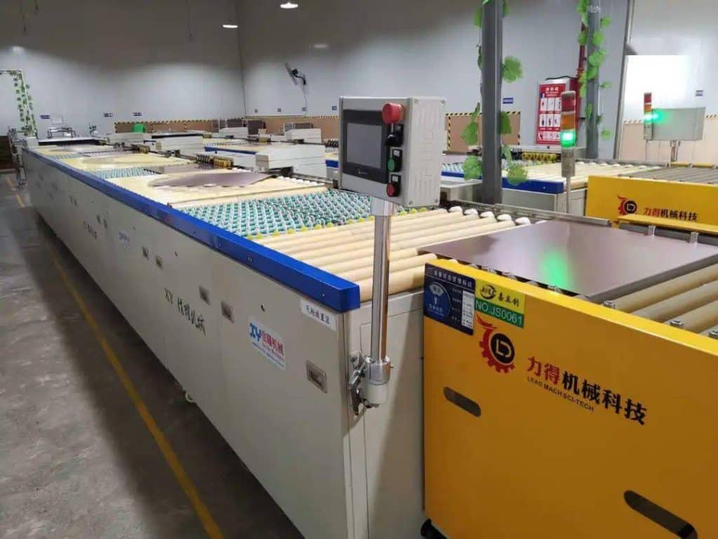
JHYPCB uses the fully automated cutting production line shown in Figure 2.
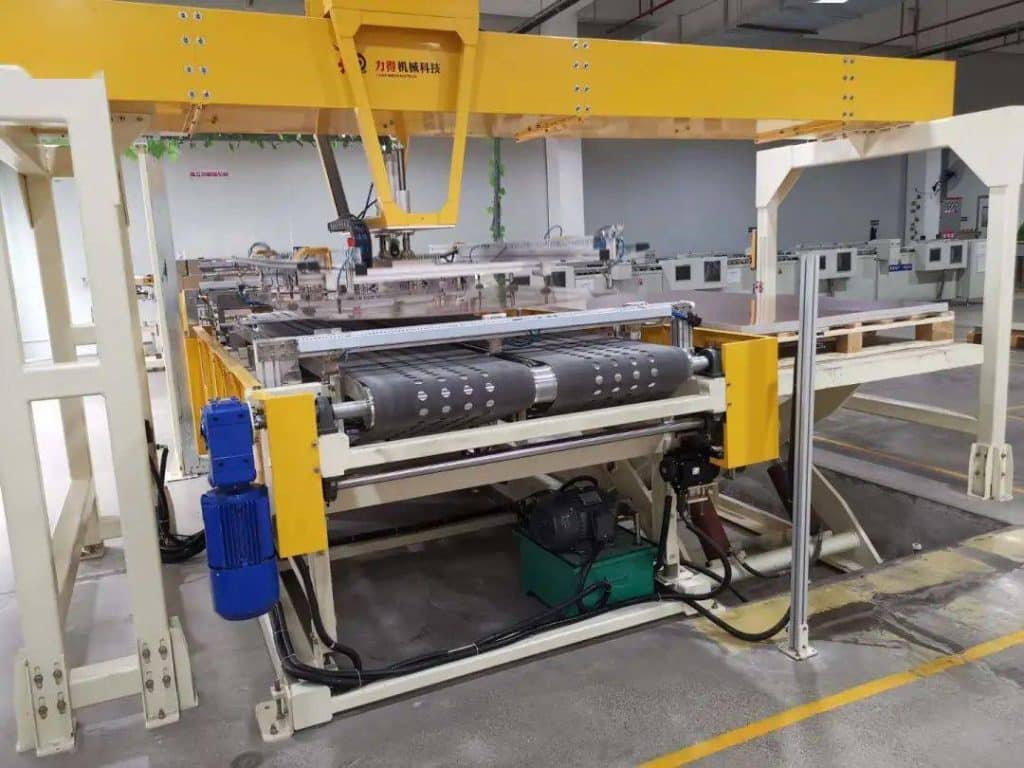
Let’s go through the entire paneling process using the example of a 49×82 inch copper foil board being cut into 690x620mm boards. On the right side of the conveyor belt in Figure 2, you can see a stack of copper foil boards waiting to be cut. At the top of the conveyor belt, you can see a copper foil board being placed onto the belt. The picking tool uses suction cups because the copper foil board surface is smooth.
As the conveyor belt moves, there will be two cutting actions — horizontally and vertically. The first cut divides the large copper foil board evenly into 3 segments, as shown in Figure 3. After the first cut, the copper foil board has been separated into 3 sections, yet it continues moving down the line. The first board in Figure 3 has moved to under the second cutting machine, which will cut it in half vertically. After the second cut, one large board has become six small boards.
The cut copper foil boards have burrs on the edges that may cause harm to production staff and machines during subsequent processes. So the edges need to be sanded down.
The paneling line already has automatic edge sanding equipment installed, as shown in Figure 4. We can see a copper foil board being automatically rotated 90 degrees by the machine. After the rotation completes, U-shaped tools sand down the edges. There will be a total of 3 rotations during the travel process, sanding down all four sides.
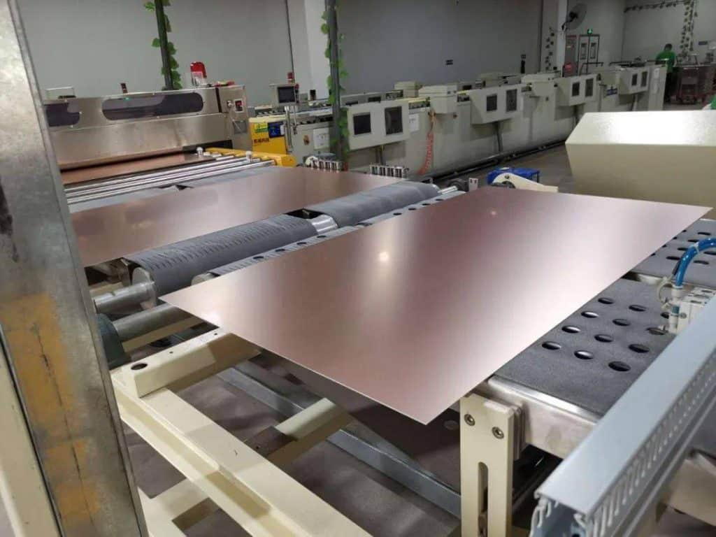
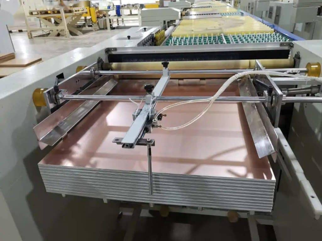
After sanding completes, the copper foil boards are automatically stacked neatly as shown in Figure 5.
Earlier we mentioned cutting the large boards into 690*620mm, 620*520mm and 620*347mm small copper foil boards. So which size exactly is needed? This is actually determined by the process table in the MI file.
The material cutting staff first print out the process table and follow the parameters there for cutting. As shown in Figure 6, this is a process table for a double-layer PCB board. In the table, we find process step No. 1 named “material cutting”. To its right it shows the required board material as FR-4, thickness 1.5mm, and panel size 690*620mm.
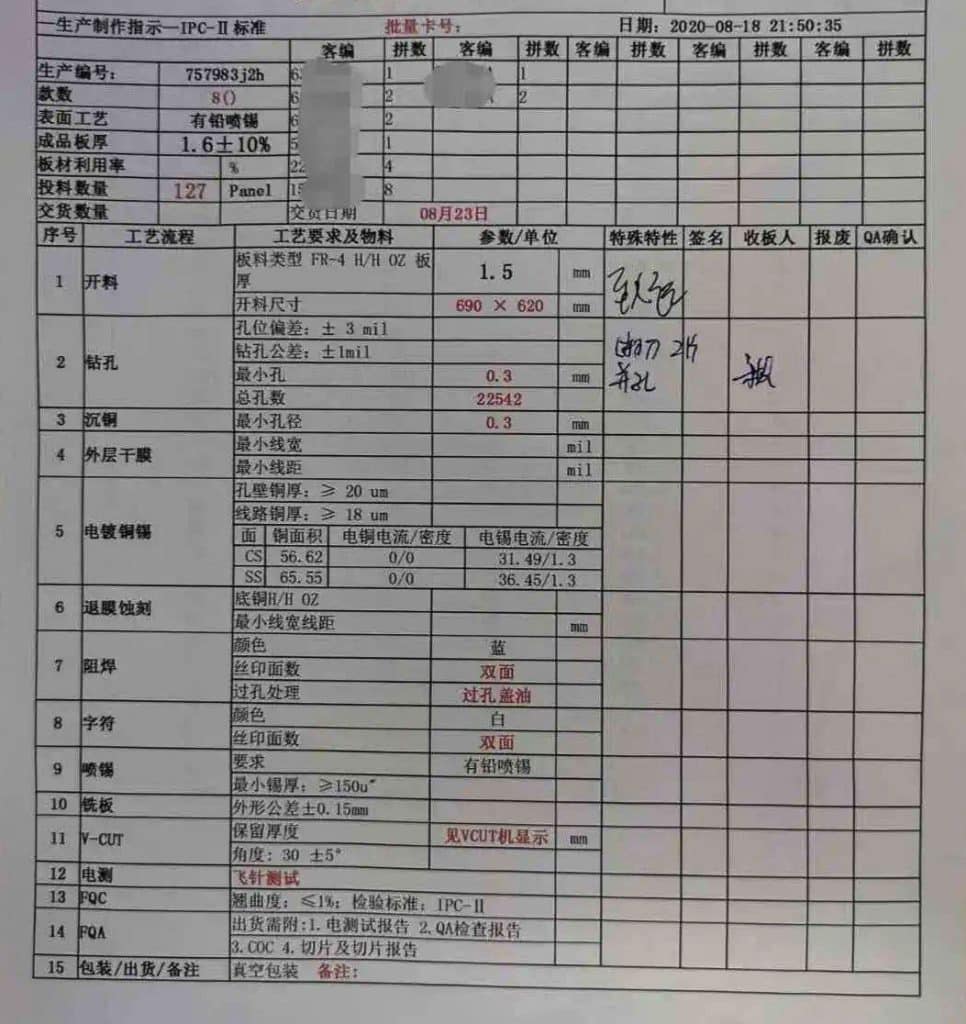
In this table, you will also come across the “Cust.” section featuring two columns. For privacy protection, I have applied mosaics in this area. The customer codes presented here correspond to your JHYPCB customer numbers, which are also imprinted on the PCB boards you receive.
By referring to these customer codes, you can discern that circuit boards for a total of 8 customers will undergo fabrication on this 690*620mm copper foil board.
This table serves as a guide for the circuit board throughout the entire production journey until it reaches the shipping stage. Each manufacturing process is obligated to adhere to the specifications outlined here.
Pinning
After the completion of the cutting process, can drilling commence? No! There is an additional step called “pinning” that precedes drilling.
Let’s consider placing such a thin copper foil board directly on the drilling machine platform and drilling holes through it. If the drill bit were to penetrate the copper foil, it would collide with the platform surface, potentially causing significant damage to the drilling machine platform. What about adding a hollow bottom support? That won’t suffice either because the copper foil board is too thin and would likely bend. Hence, the need arises to place a relatively thick paper board beneath the copper foil board. If you’ve ever ordered solder masks from JHYPCB, you might have encountered this board — when shipped, solder masks are safeguarded by two of these boards. The paper board will also be visible in the upcoming images.
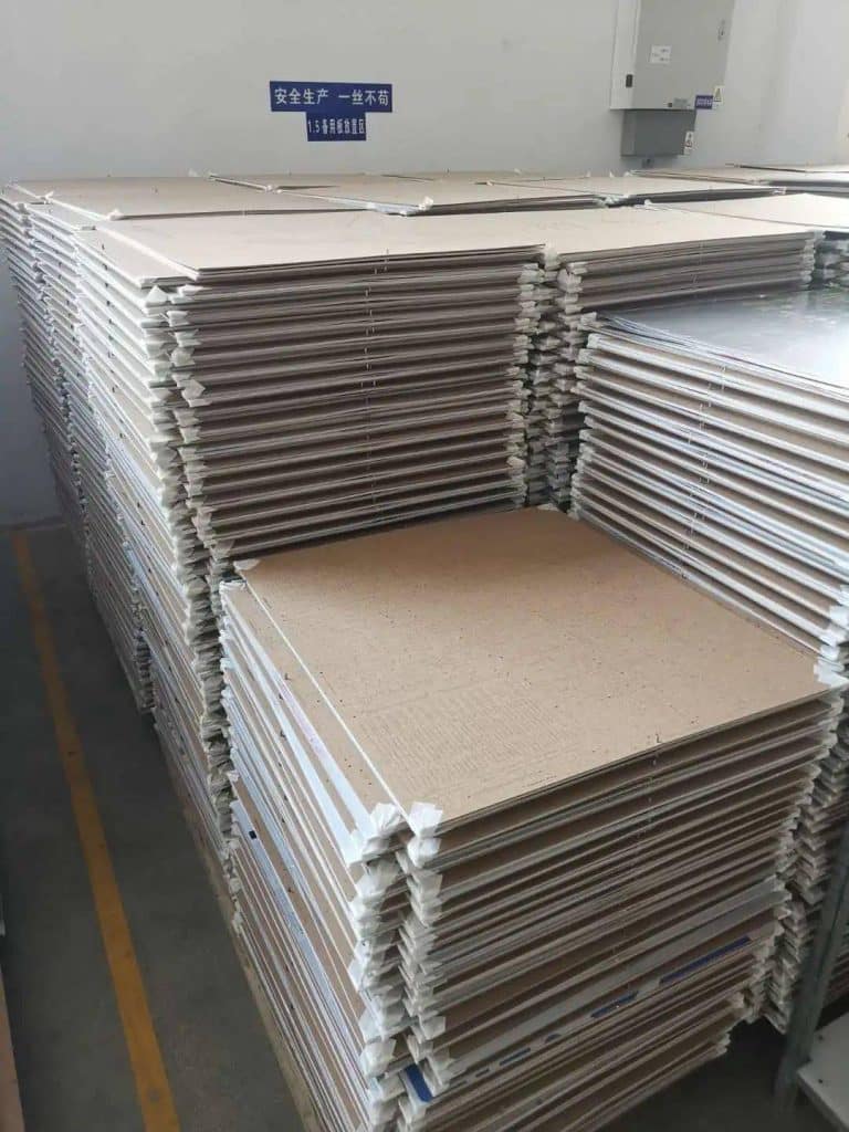
To enhance production efficiency, JHYPCB drills several stacked copper foil boards simultaneously. The number of boards stacked depends on the foil thickness. For instance, 1.5mm boards, post-paneling, would be stacked in threes, with the mentioned paper board at the very bottom, forming the entire stack.
To prevent issues such as shifting and misalignment during drilling, which could lead to the fabrication of non-functional boards, it is crucial to secure the stacked boards properly. This is precisely why the aforementioned “pinning” step is essential.
Figure 7 illustrates a JHYPCB staff member using a pinning machine to secure the copper foil and paper boards.
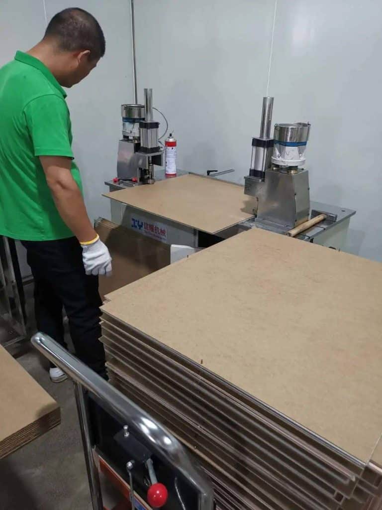
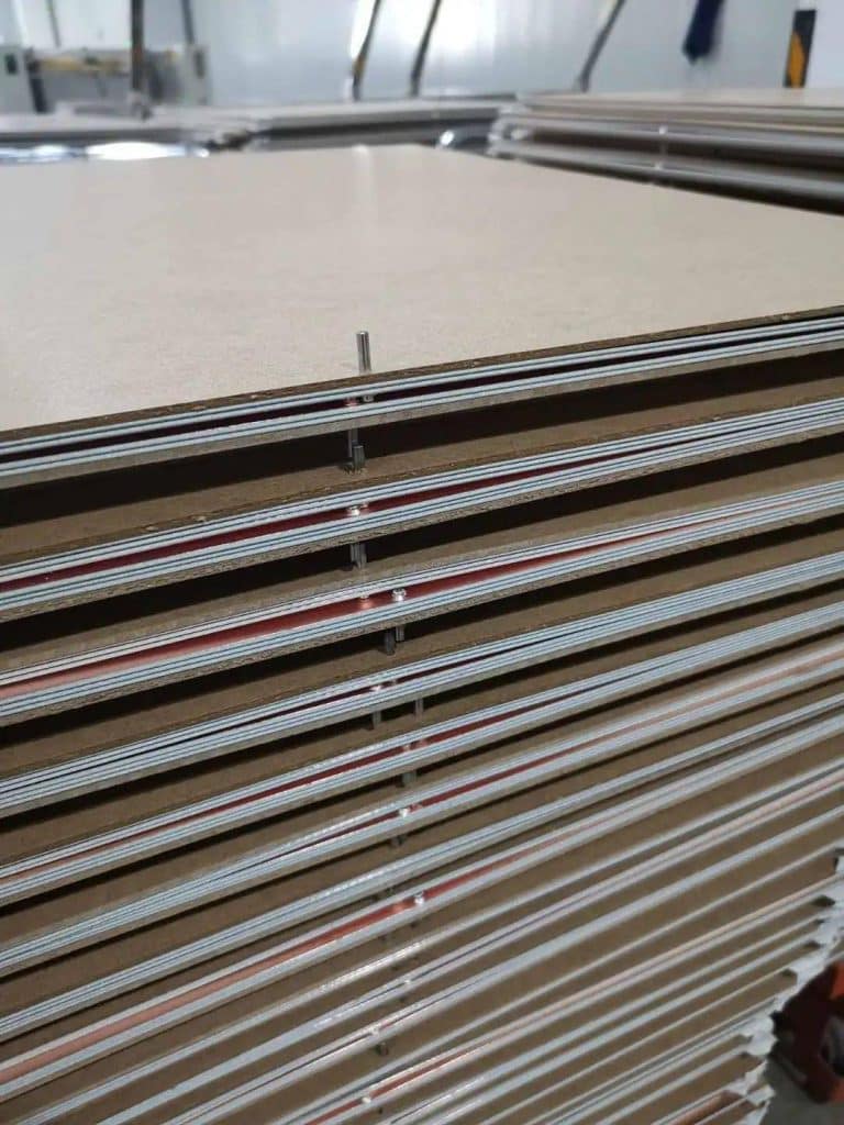
Figure 8 shows pinned copper foil and paper boards ready for drilling.
Let’s look at some details here — Figure 9 shows that besides securing the boards to prevent shifting, the pins also serve to fix the copper foil board onto the drilling machine platform.
Drilling
So far we have introduced the “cutting” and “Pinning” steps. Now we officially enter the “Drilling” stage.
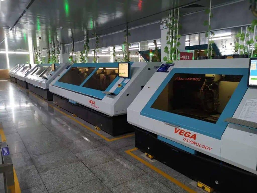
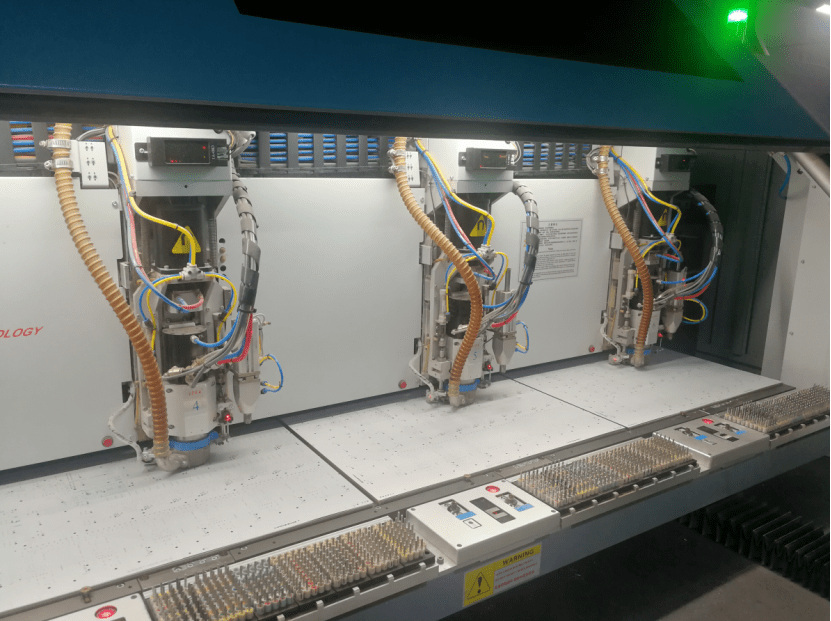
Figure 10 shows a drilling machine used at JHYPCB.
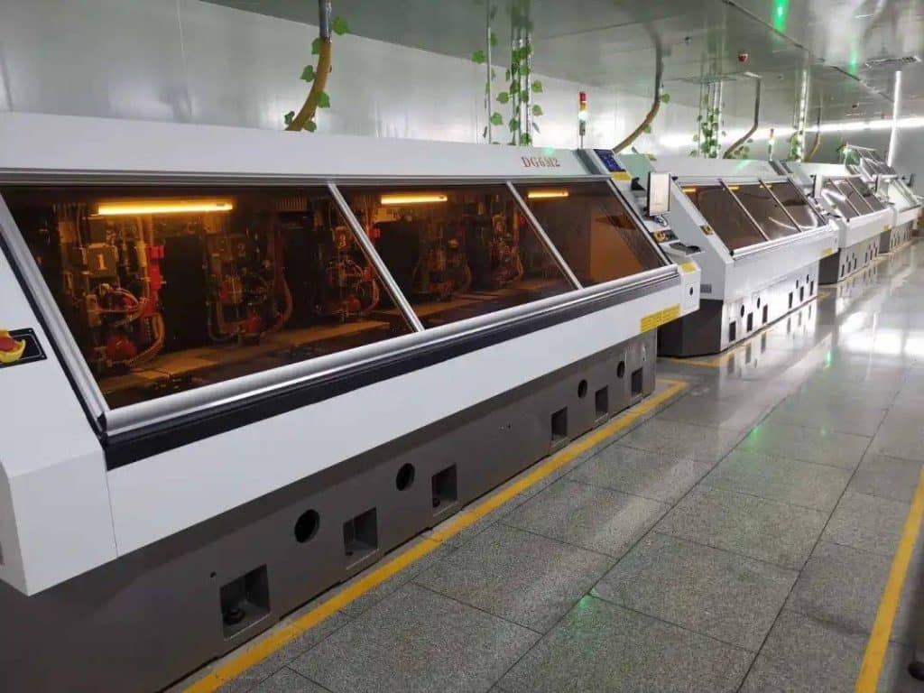
Figure 11 shows a VEGA drilling machine used at JHYPCB.
In Figure 11 below the drilling machine’s computer screen there is a paper — this is the process table mentioned earlier. It contains a production ID number. You can cross check it with the process table introduced previously. Enter this production ID into the drilling machine computer to call up the corresponding drilling parameter file from the MI file. With this parameter file, the drilling machine knows exactly which positions on the copper foil board need drilling.
Before the drilling operation begins, the pinned copper foil and paper boards need to be fixed onto the machine platform, with paper board at the very bottom. There will also be a sheet of aluminum placed on the very top. The aluminum sheet serves two purposes: cushioning the drill bit for more even drilling holes, and helping with heat dissipation to prevent drill bit overheating.
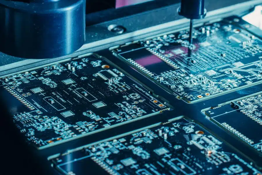
As mentioned previously, the drilling process opens holes of all required hole sizes on the PCB board. There can be many different hole sizes in our designed circuit boards, so the drilling machine needs to be equipped with drill bits of many diameters. Figure 12 shows a running drilling machine — you can see the neatly arranged drill bits in front of the workstation.
These drill bit diameters range from 0.2mm, 0.25mm, 0.3mm…, incrementing by 0.05mm. Every hardware engineer has different design habits and preferences. Different products also have diverse design requirements. As a result, a copper foil board needs the involvement of drill bits with multiple hole sizes.
Each drill bit needs to be maintained and sharpened after drilling a certain number of holes, otherwise the precision decreases. Specifically, how often maintenance is needed depends on the hole size — larger bits can drill more holes before needing maintenance. For example, a 0.3mm bit needs maintenance after drilling 3000 holes in a double-sided board, while a 3mm bit requires maintenance after 800 holes.
Next to the drill bits you can see there is a laser detector in Figure 12 that automatically checks if each drill bit meets requirements after the machine selects one for use. Once cleared, it starts drilling the particular sized holes. When all such holes are completed on the board, the machine swaps in the next bit. JHYPCB has a specialized workshop dedicated to drill bit maintenance and sharpening.
After drilling fully completes, the machine auto reports completion to the server.
With the drilling step done, the boards move to the next process: Plating!


