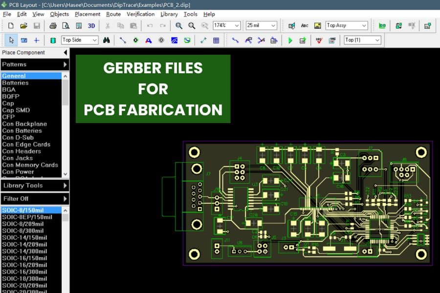
When discussing PCB prototyping, accurately conveying PCB design data is imperative. As the industry-standard file format, Gerber files play a pivotal role in this process.
However, many engineers often make big and small mistakes when preparing these critical files. So what are some easily overlooked details about Gerber files? And how do they impact prototype quality? What key points should you watch out for when generating these files?
This guide answers these questions fully, offering an insider’s peek into the mysterious world of Gerber files. We’ll focus on:
- Gerber file format specifications
- Workflows for different layer type files
- Naming conventions
- File integrity checks
- Common error case studies
- Standard procedures for submitting files to PCB manufacturers
With comprehensive analysis and real-world examples, this guide aims to be your best reference for flawless Gerber file preparation – unlocking design intent to ensure optimal PCB prototyping quality!
Table of Contents
Gerber File Formats
When generating Gerber files, the first key decision is selecting the right output format from your CAD software.
Historically, the RS-274D specification published by Gerber Systems Corporation has been dominant. This uses 2D vector coordinates to represent PCB geometry like trace outlines, pads, and holes.
However, in recent years, an enhanced format called RS-274X has grown popular. It extends RS-274D’s capabilities to support newer features like step-and-repeat, regions, netlist data and embedded component information. This enriched metadata helps PCB manufacturers select optimal processes.
Another modern option is the ODB++ format that encodes design intent even more comprehensively. It stores the native data structures of EDA tools allowing more facets to be conveyed compared to Gerber files.
So which option should designers choose? For most common applications, RS-274X strikes a good balance between universality and increased intelligence. It’s backwards compatible for older equipment while embedding richer semantics to guide factory optimization. But for very advanced designs, ODB++ is preferred.
In summary, RS-274X enhances 2D Gerber’s legacy status as the lingua franca of PCB prototype fabrication for much of the industry currently when exported from CAD systems.
Layers Types and Outputs
Gerber files represent different types of CAD layers in the PCB design. It’s critical to understand the purpose and preparation requirements for each.
Signal layers like copper and silkscreen directly influence circuit functionality and visuals. The conductors and component outlines must be rendered correctly.
In contrast, non-signal layers serve auxiliary functions like board demarcation or milling instructions. Examples include the soldermask, outline, and drill/tooling layers.
Another vital concept is positive vs negative plots. All conductors and pads must employ positive polarity while dielectric backgrounds use negative polarity. This ensures precise imagery between layers.
When generating files, designers must be aware of options that impact final visual appearance like using a minimum stroking width or clipping surface designs to the board profile.
In summary, appreciating the workflow nuances between signal and non-signal layers coupled with positive/negative considerations is an important starting point for flawless prototype fabrication.
File Naming Conventions
Standardized file naming conventions are crucial for avoiding mismatches when assembling all the Gerber layers during CAM processing.
Experts recommend employing a consistent naming schema that captures critical details like:
- Board project name
- Layer type (Top Copper, Bottom Soldermask etc.)
- Polarity (Positive or Negative)
- Design revision version
- File creation date
For instance, a robust file name could be:
PCBPrototype_BottomCopper_Positive_Rev2_20231124
Some other guidelines include:
- Using short file names without special characters
- Specifying units like MM or INCH
- Adding author/engineer initials
- Assigning numbers to inner layer names
Adhering to these naming best practices prevents incorrect layer stack-ups, alignments issues and component misplacements during PCB prototyping fabrication.
A diligent naming system goes hand-in-hand with understanding layer type preparations for ensuring correctness.
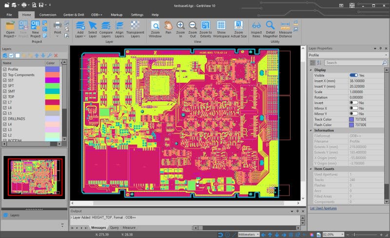
Certainty Through Visual Validation
Once all the Gerber files are generated, smart engineers visually validate the layer alignments before shipping to manufacturers.
Simple software viewer tools like GerbView, Pentalogix ViewMate, and Ucamco’s GerbView let designers overlay all copper, soldermask and silkscreen files in a stackup to perform sanity checks. This reveals errors like:
- Pads or vias not cleared of soldermask
- Exposed copper not fully covered by mask
- Component markings outside allowable print bounds
More advanced DFM analysis software like Valor MSS’s Fabrication Preparation tool automatically flag common problems too while displaying visual violations. This helps designers rectify issues like validations against a customized manufacturing rule deck.
Lastly, an integrated layer-by-layer final check before combining everything into the final ODB++ output removes any lingering concerns.
This expert practice of “trust but verify” before submitting files instills confidence that all layers will align perfectly during prototyping fabrication for the highest quality.
Validating File Integrity
While visual checks enable fixing obvious errors, further programmatic validation should occur to capture difficult problems like inadvertent subsumption or accidental polygon pouring that may escape ocular detection.
Designers can leverage validation capabilities offered within CAD systems themselves to thoroughly interrogate file integrity from multiple lenses:
Electrical Rules Check (ERC)
Strictly confirms if schematic connectivity intents translated accurately into board layout especially for complex multi-channel high-speed designs. Flags shorts, opens and missing connections.
Geometric Review
Checks if minimum spacing rules or component enclosures have been breach because of overlapping copper or silkscreen graphics.
Connectivity Verification
Validates if connected nets have consistent naming and electrical properties through the entire design database especially crucial for dense BGAs/QFNs packages prone to hidden breaks.
Layer Integrity Audits
Inspect if each layer contains the exact required contents and boundary extents with no accidental exclusions or artifacts.
Together these audits comprehensively vet the files from multiple significant perspectives quickly spotlighting hard flaws. Fixing these avoids damaging downstream prototype surprises and maintains fidelity to the original design vision.
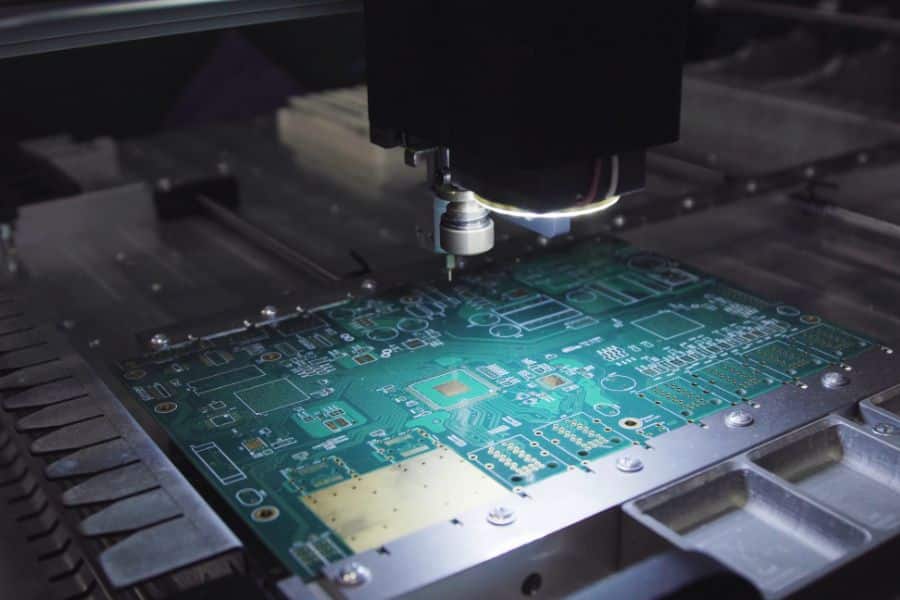
Submitting Files to Your Manufacturer
Once all necessary Gerber files have been generated and thoroughly checked, smart preparation also involves proper packaging and transfer protocols when providing to your chosen prototyping partner.
Experts recommend compressing all files into a single ZIP archive with intuitive project naming conventions like ProductX_Rev2_GerberFiles. This guarantees all relevant files are bundled together avoiding confusion or questions.
Share transfer links securely using services like WeTransfer for large payloads ensuring reliable downloads. For extra precaution, discuss checksums with your vendor for them to validate file completeness accurately after transfer.
If iterations occur, adopt sequential versioning like _V01, _V02 for related sets of changed files. Maintain clear traceability this way.
Also finalize any special instructions required using a PIDX manufacturing info form highlighting applicable soldermasks, surface finishes, material types, tolerances or other supplementary specifications for your board.
These administrative best practices will serve you well over multiple prototype cycles with your fabrication ally, ensuring smooth transfers and timely fabrication.
Learning From Insidious Errors
Creating flawless Gerber files is never as easy as it seems. Even seasoned designers often get checkmated by their oversight.
The most common is forgetting to include an essential layer’s data, or missing out vital labels for layer name or polarity. Such deviations lead to garbled routing plots or worse, near unusable prototypes at the extreme.
An insidious gotcha is generating humongous copper pours thanks to inadvertent polygon fills that gobbled up the entire bottom plane as reference. Not only does this waste material, it also invites thermal stress headaches. Saddening war stories fill the C.H.I.P. chamber of Silent CAM even from veterans.
Even fiducials markers bite back when least expected. Despite believing safeguards exist to prevent overlaps into active areas, they somehow transform into patchwork eyesores when soldermasks get applied and post-processed.
These lessons teach us about infinite ways to botch the job despite checklists to the contrary! So never take short-cuts by avoiding completeness checks and visual validations before submission.
Conclusion
We hope this comprehensive guide has illuminated what excellence looks like for Gerber files intended for flawless PCB prototyping. While intricate details constrain options, awareness of recommended practices liberates engineers to exercise sufficient diligence during preparation.
As your dependable Chinese manufacturing partner renowned for quality and speedy delivery through cutting-edge infrastructure, JHYPCB is ready to fabricate those meticulously designed prototypes smartly conveyed through perfect Gerber files. Our online DFM checks further reinforce your validation efforts.
Let’s keep perfecting processes together across upcoming projects on the quest for prototyping perfection! Please feel free to contact us at sales@pcbjhy.com for quotes.
Related Reading