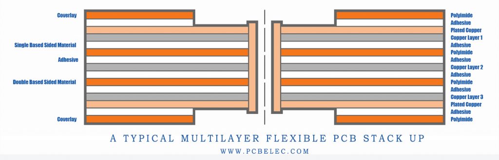
The stack-up of a multilayer PCB is essential. As there can be many layers, it is essential to understand how they are stacked. It is generally preferred to have an even number of layers in a multilayer PCB as it creates symmetry around the middle core layer. An odd number of layers is possible and still required in some applications, but even layers are preferred as they have more physical strength due to symmetry.
The stack-up in a multilayer PCB is quite simple. The inner layers are like double-layer PCBs, and the surface layers are like single-layer PCBs. It might be challenging to understand in the first place, but it is pretty simple.
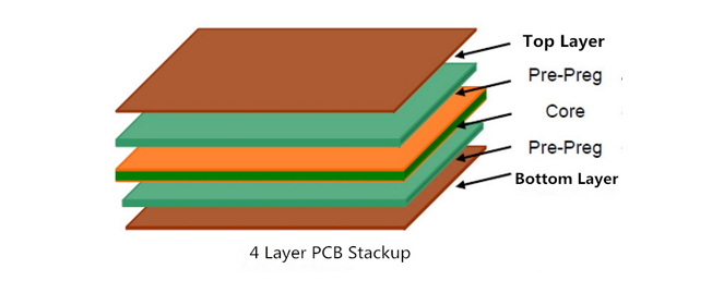
Suppose there is a 4-layer PCB. The middle layer of the PCB will be the core layer. On both sides of the core, there will be conductive layers. This is just like a double-layer PCB. Now, there will be an insulation layer, prepreg, above these two layers. After that, there will be surface layers, one at the top and one at the bottom. These two layers are like a single-layer PCB. It means a 4-layer PCB has one double-layer PCB and two single-layer PCBs. As the number of layers increases, the number of double-layer PCBs increases, while the number of single layers remains constant; only two single layers.
What is Stack-up in a Multilayer PCB?
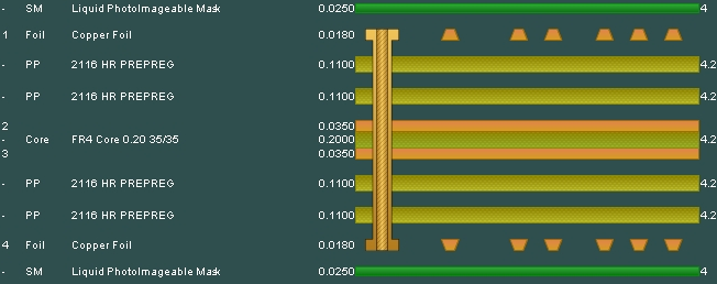
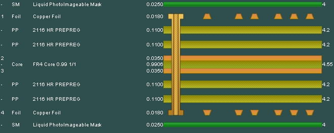
4 Layers PCB Stackup and Thickness
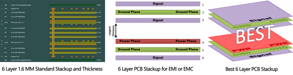
6 Layer PCB Stackup and Thickness
8 Layer PCB Stackup and Thickness
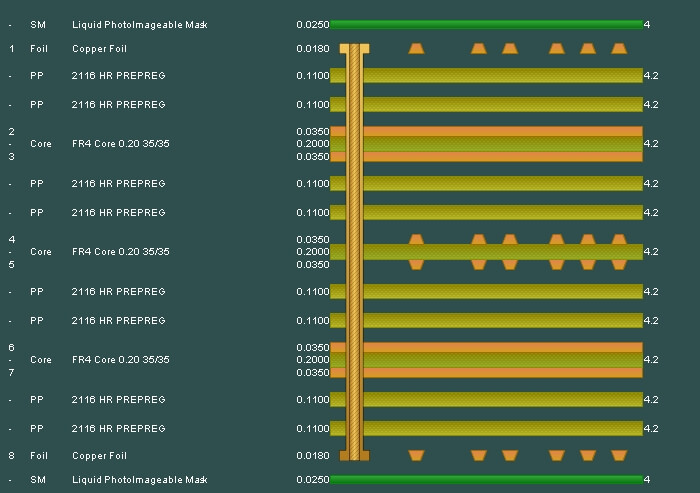
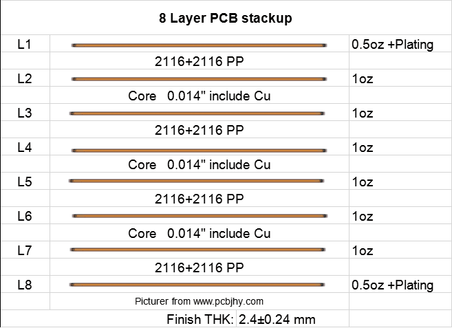
The above image explains the stack up in an 8-layer PCB. There are three cores in the PCB, and each core has two conductive layers. After every conductive layer, there is a prepreg layer for insulation. Finally, there is a surface layer at the top and one surface layer at the bottom. The components are placed on the surface layers only.
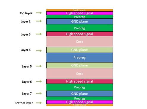
The stack-up remains the same in all multilayer PCBs; only the number of double-layer cores increases. Moreover, it is up to the user which layer he chooses for power, ground, signal, or any other purpose.
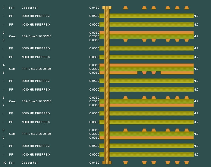
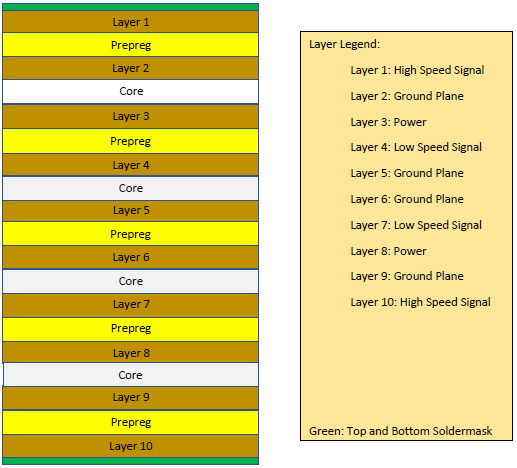
10 Layer PCB Stackup and Thickness
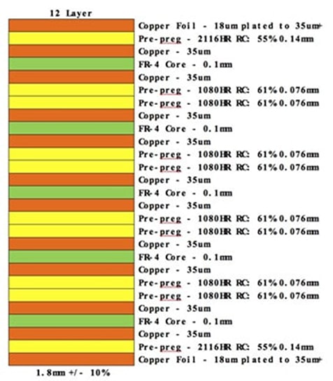
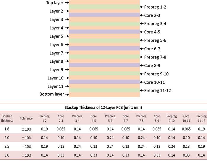
12 Layer PCB Stackup and Thickness
How are Layers Connected in Multilayer PCB?
The stack-up of the layers is clear, but the question that comes to mind is about the connection of these layers. These layers can be interconnected with all layers or a few selected ones. As the layers are stacked up one over the other, having insulation between them, the only way to connect them is vias.
Via can connect the layers of the PCB. It is actually a hole created to make a connection between the layers. The hole can be for the connection of two layers, three layers, or as many as you need. A hole is created in the PCB, and its walls are plated so that it can create a connection.
Primarily, there are three types of vias used in PCB.
1. Plated Through Hole (PTH)
2. Blind Via
3. Buried Via
PTH is the simple type of via that joins all layers together. It is just like drilling the PCB until the drill bit comes out from the other side. After drilling, the hole is plated so that connections can be made.
Blind via can be seen from one side because it creates the connection of the surface layer with any layer present under it. It can be used to create a connection with internal layers, and there can be one or more internal layers.
Buried vias are buried under the PCB. They are not visible from either side. These vias create a connection between the inner layers only. Thus, these are the most complicated vias.
According to the connections, the PCB layers are arranged. The vias are created as per the requirement. For the plating of via, the board is drilled and then cleaned to remove the dust and debris. A thin layer of copper is applied first. Then, the board is passed through an electroplating process. There are a series of chemical and electroplating baths. After this process, the vias create a connection between the layers.
Learn more about Plated Through Hole, Blind Via, and Buried Via in PCB Fabrication
Specialized Equipment for Pressing Multilayer PCB Circuit Boards
PCBs Manufacturing multilayer PCBs requires a specialized hydraulic press with heated platens. Initially, the books are squeezed with a “kiss” pressure of 50 psi before being heated to 350F at 350 psi for a minimum of one hour. The assembly is then allowed to cool slowly before removal for further processing. At Omni, the maximum size of a multilayer board is “12×16″ while the board thickness can range from 0.015″to 0.125”.
Multilayer PCBs Fabrication Process
The outer layers of the multilayer consist of sheets of glass cloth pre-impregnated with uncured epoxy resin (prepreg) and a thin copper foil.
The PCB material brands available are Rogers, Shengyi, Dupont (for multilayer flexible PCB), KB (King board), Arlon, Isola, ITEQ, EMC, etc.
For more information about PCB materials, you can read the following articles.
- What Is FR-4 Material In PCB Fabrication?
- Why choose FR4 as the general material of PCB?
- What is the Tg value of PCB substrate?
- Why is FR4 Used to Make High Tg PCBs?
The lay-up operator has already placed a copper foil and two prepreg sheets on the heavy steel baseplate. Now he sets the pre-treated core carefully over the alignment pins. Then he adds two more layers of prepreg, another copper foil, and an aluminum press plate.
He builds up to three panels on the baseplate in the same way. Then he rolls the massive stack under a press which lowers down the steel top plate. He pins the stack together and runs the finished stack out of the cleanroom into a rack.
The press operator collects three stacks on a loader and loads them into the bonding press. This press uses heated press plates and pressure to bond the PCB layers together. The heat melts and cures the epoxy resin in the prepreg while the pressure bonds the PCB together. The process is computer controlled to build up the heat and the pressure correctly, hold it, and cool the press down. In this way, we ensure a permanent bond that will last the lifetime of the PCB. Our board has four layers, but complex PCBs for defense, avionic, and telecommunications applications can have more than 50. These may include sub-assemblies of cores, prepregs, and foils drilled and plated before being assembled into the final PCB.
Once the cycle is completed, the press operator unloads the press and carefully rolls the massive stacks into the cleanroom. Here the lay-up operator de-pins the stack and removes the top plate. He unloads each panel from the stack, eliminating the aluminum press plates used to ensure a smooth copper finish. The copper foil is now bonded in place to form the outer layers of the PCB.
For more step-by-step introduction to the PCB manufacturing process, please click here.
Recommended Reading
Multilayer PCB Manufacturing Videos
Quality Standard and Control of Multilayer Printed Circuit Board
The manufacturing of multilayer PCB requires perfection in every step to ensure the quality of the final product. The following are the IPC standards for multilayer PCB manufacturing.
| IPC DOC# | ITEMS | Publication date |
| IPC-L-108 | Specification for Thin Metal Clad Base Materials for Multilayer Printed Boards | Jun-90 |
| IPC-L-109 | Specification for Resin Impregnated Fabric (Prepreg) for Multilayer Printed Boards | Jul-92 |
| IPC-CC-110 | Guidelines for selcting core constructions for multilayer printed wiring board applications | Dec-97 |
| IPC-TR-470 | Thermal Characteristics of Multilayer Interconnection Boards | Jan-74 |
| IPC-TA-721 | Technology Assessment Handbook on Multilayer Boards | |
| IPC-HM-860 | Specification for Multilayer Hybrid Circuits | Jan-87 |
| IPC-ML-960 | Qualification and Performance Specification for Mass Lamination Panels for Multilayer Printed Boards | Jul-94 |
| IPC-4101E | Specification for Base Materials for Rigid and Multilayer Printed Boards | Mar-17 |
Click here to learn more about PCB IPC standards.
How To Store Multilayer PCBs?
The packaging and storage of printed circuit boards have strict requirements. The storage and shelf life of multilayer PCBs are specified in the IPC standard. Foam cotton and vacuum packaging are required for packaging.
Related Reading: How to Store PCB and PCBA?


