sales@pcbjhy.com

Sales Manager: Ms. Megan

+86-13825274100

24/7 Customer Support

+86-13825274100

WeChat and WhatsApp

Guide to Multilayer PCB Layer Stackup and thickness

PCB Stack-up refers to the arrangement of copper layers and insulating layers that make up a PCB prior to board layout design. PCB stack up is am important part of the PCB design and manufacturing process.

What is PCB stack-up?

PCB Stack-up refers to the arrangement of copper layers and insulating layers that make up a printed circuit board prior to board layout design.

For multi-layer PCB, PCB layers include Ground Plane (GND Plane), Power Plane (PWR Plane), and Inner Signal Layers. The layer distribution in the printed circuit board conforms to a symmetrical or balanced structure. In addition to layer layout, PCB designers and PCB manufacturers should also take the spacing between layers seriously. To meet the miniaturization requirements, minimum trace spacing must be obtained when planning the layer stack. The space between the layers can be the core material or the prepreg. Multilayer boards typically consist of at least one or more cores and prepregs. The core material consists of copper-plated glass fiber reinforced epoxy resin laminates. The thickness of the core material is between 0.1mm and 0.3mm.

PCB Layer Stack up

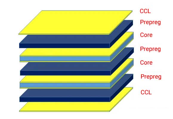
Prepreg is a general term for reinforced fabrics pre-impregnated with resin systems. Such resin systems (usually epoxy resins) already contain suitable curing agents. The primary function of the prepreg is to stack all the layers into a whole board by high temperature. The table below shows the physical and chemical properties of the prepregs (7628, 2116, and 1080).

According to different application scenarios and needs, the thickness of prepreg is also different. Factors including inner layer thickness, product design thickness requirements, manufacturing process limitations, actual performance, and actual thickness after stackup must be considered when determining the amount of prepreg.

Why stack up?

Modern electronic products are increasingly developing towards miniaturization, lightweight, high speed, and integration, requiring more functions, higher reliability, and longer service life, which has led to many applications of multilayer PCBs. We all know that a multilayer PCB usually has three or more conductive layers. As multilayer PCB designs become more complex and denser, problems such as noise, stray capacitance, and crosstalk may arise when the layers are not properly arranged.

Planning optimal multilayer stack-up is one of the most critical elements in determining a product’s Electromagnetic Compatibility (EMC) performance. A well-designed layer stack-up can minimize the radiation and stop the circuit from interfering with by external noise sources. Well-stacked PCB substrates can also reduce signal cross-talk and impedance mismatch issues. However, an inferior stack-up may get EMI (Electromagnetic Interference) radiation rising because reflections and ringing in the system due to impedance mismatch can dramatically lower products’ performance and reliability.

The stackup JHYPCB typically uses for standard PCB fabrication services is shown below. The actual layer stackup will be determined by the PCB material and other desired factors. If you have special requirements for multi-layer PCB layer stackup, please email your board thickness and number of layers for consultation.

4 Layer PCB Stack up and Thickness

4 layer PCB stackup
4 Layer PCB Stack up-0.6mm of board thickness
4 layer PCB stackup - 0.8mm board thickness
4 Layer PCB Stack up - 1.0mm of Board Thickness
4 Layer PCB Stack up - 1.2mm of Board Thickness
4 Layer PCB Stack up - 1.6mm of Board Thickness
4 Layer PCB Stack up - 2.0mm of Board Thickness
4 Layer PCB Stack up - 2.2mm of Board Thickness
4 Layer PCB Stack up - 2.4mm of Board Thickness
4 Layer PCB Stack up - 2.6mm of Board Thickness
4 Layer PCB Stack up - 2.8mm of Board Thickness
4 Layer PCB Stack up - 3.0 mm of Board Thickness
4 Layer PCB Stack up - 3.2 mm of Board Thickness

6 Layer PCB Stack up - 0.8 mm of Board Thickness

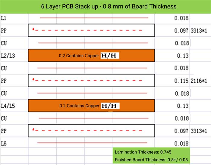
6 Layer PCB Stack up – 0.8 mm of Board Thickness

6 Layer PCB Stack up - 1.0 mm of Board Thickness

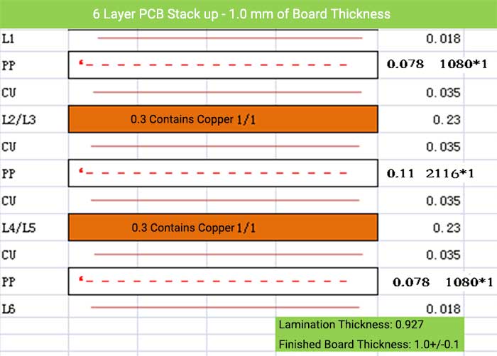
6 Layer PCB Stack up – 1.0 mm of Board Thickness

6 Layer PCB Stack up - 1.2 mm of Board Thickness

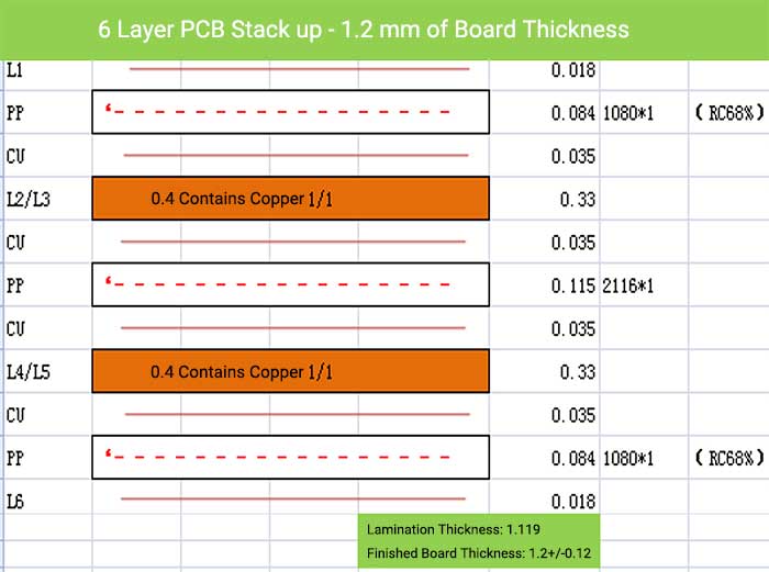
6 Layer PCB Stack up – 1.2 mm of Board Thickness

6 Layer PCB Stack up - 1.6 mm of Board Thickness

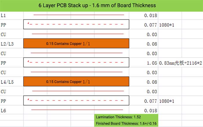
6 Layer PCB Stack up – 1.6 mm of Board Thickness

6 Layer PCB Stack up - 2.0 mm of Board Thickness

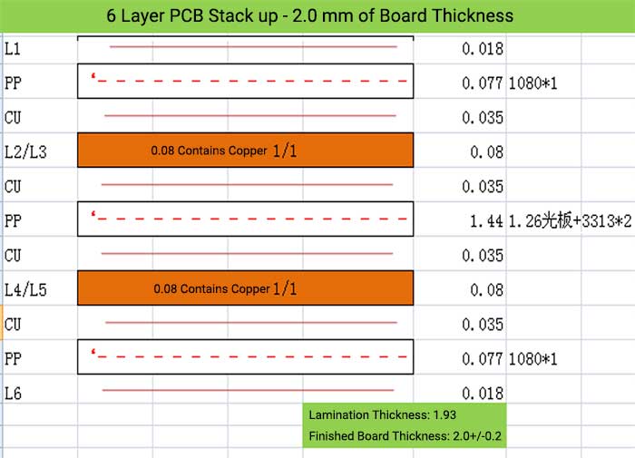
6 Layer PCB Stack up – 2.0 mm of Board Thickness

6 Layer PCB Stack up - 2.2 mm of Board Thickness

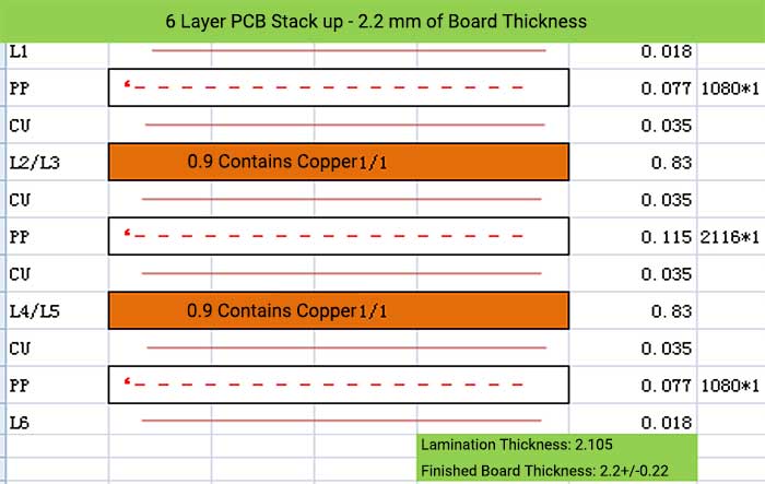
6 Layer PCB Stack up – 2.2 mm of Board Thickness

6 Layer PCB Stack up - 2.4 mm of Board Thickness

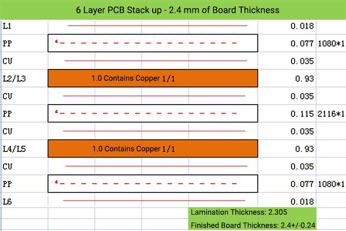
6 Layer PCB Stack up – 2.4 mm of Board Thickness

6 Layer PCB Stack up - 2.6 mm of Board Thickness

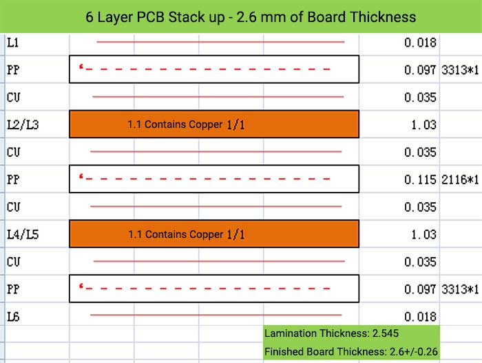
6 Layer PCB Stack up – 2.6 mm of Board Thickness

6 Layer PCB Stack up - 2.8 mm of Board Thickness

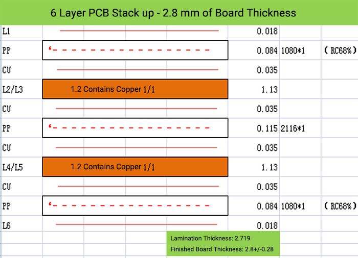
6 Layer PCB Stack up – 2.8 mm of Board Thickness

6 Layer PCB Stack up - 3.0 mm of Board Thickness

6 Layer PCB Stack up – 3.0 mm of Board Thickness

6 Layer PCB Stack up - 3.2 mm of Board Thickness

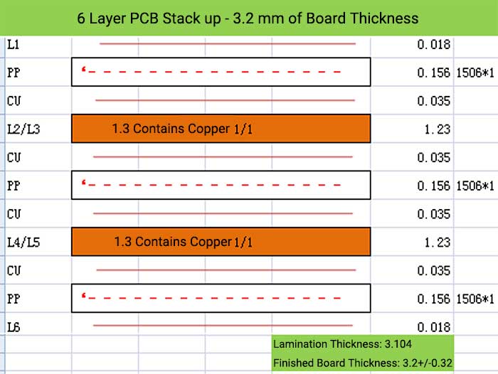
6 Layer PCB Stack up – 3.2 mm of Board Thickness

8 Layer PCB Stack up - 1.0 mm of Board Thickness

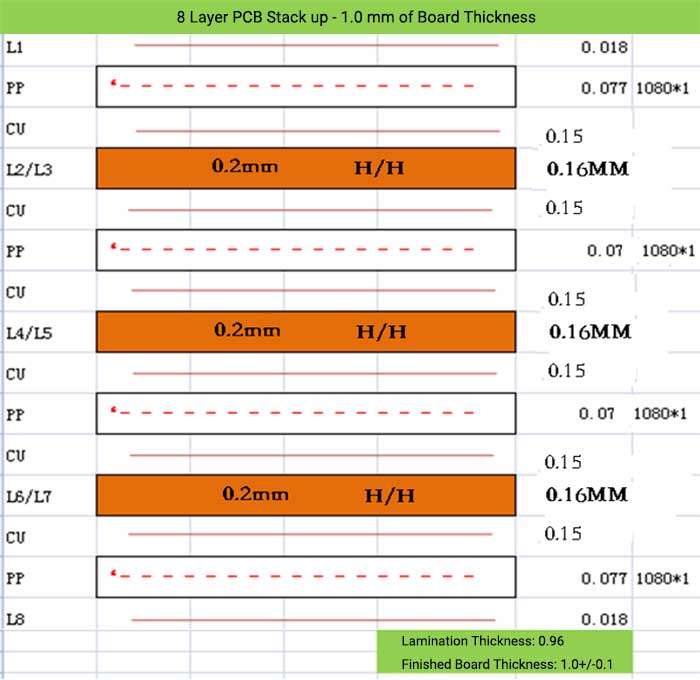
8 Layer PCB Stack up – 1.0 mm of Board Thickness

8 Layer PCB Stack up - 1.2 mm of Board Thickness

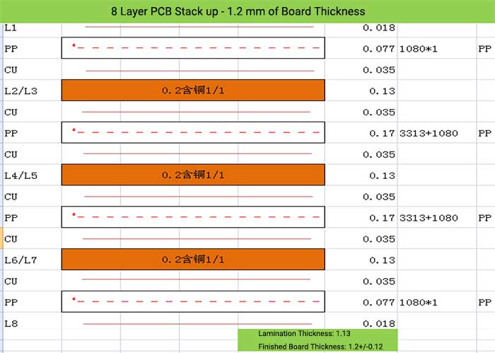
8 Layer PCB Stack up – 1.2 mm of Board Thickness

8 Layer PCB Stack up - 1.6mm of Board Thickness

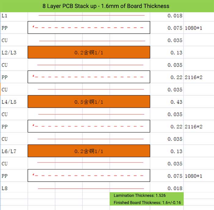
8 Layer PCB Stack up – 1.6mm of Board Thickness

8 Layer PCB Stack up - 2.0 mm of Board Thickness

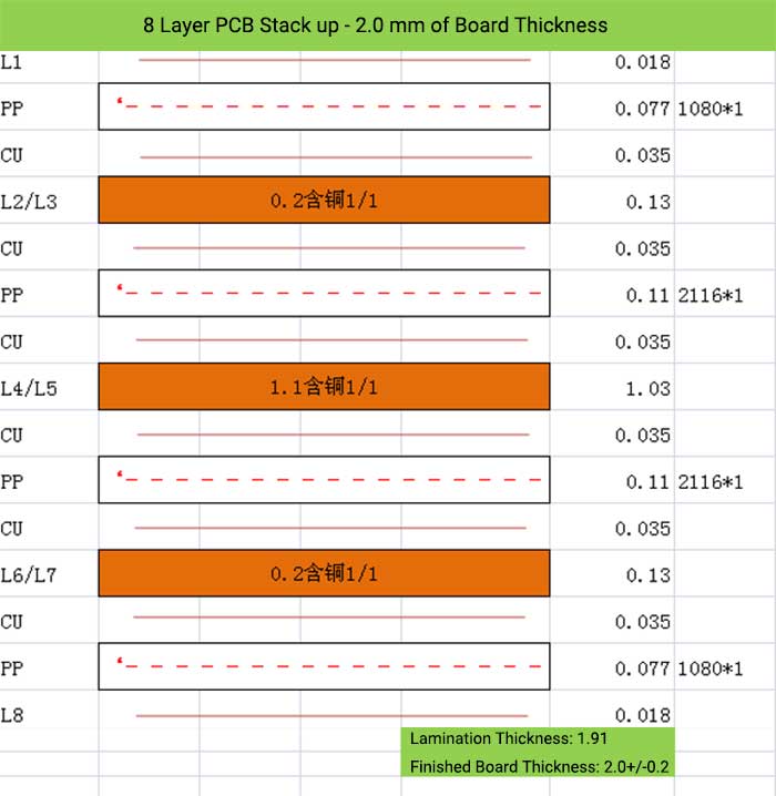
8 Layer PCB Stack up – 2.0 mm of Board Thickness

8 Layer PCB Stack up - 2.2 mm of Board Thickness

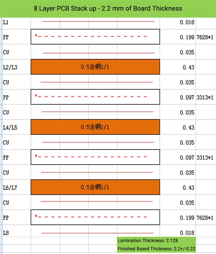
8 Layer PCB Stack up – 2.2 mm of Board Thickness

8 Layer PCB Stack up - 2.4 mm of Board Thickness

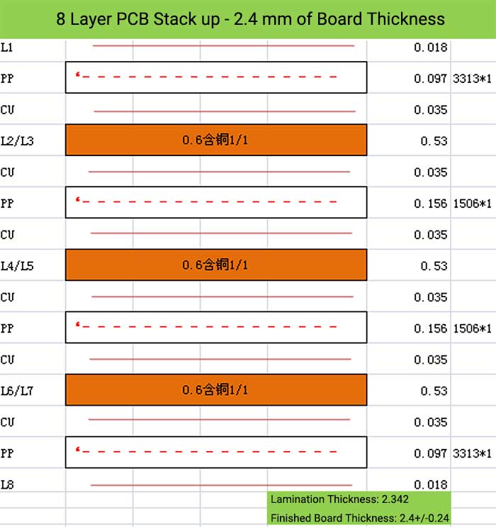
8 Layer PCB Stack up – 2.4 mm of Board Thickness

8 Layer PCB Stack up - 2.6 mm of Board Thickness

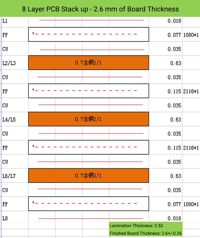
8 Layer PCB Stack up – 2.6 mm of Board Thickness

8 Layer PCB Stack up - 2.8 mm of Board Thickness

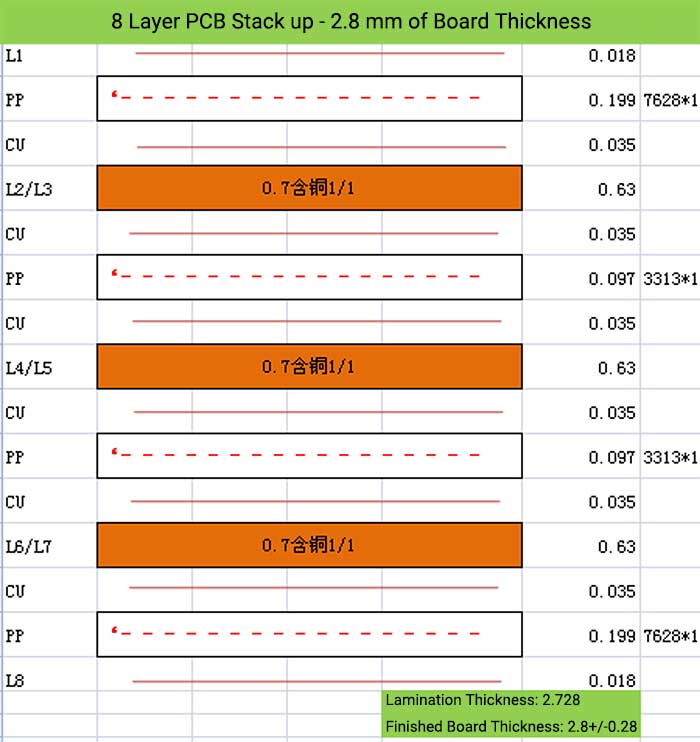
8 Layer PCB Stack up – 2.8 mm of Board Thickness

8 Layer PCB Stack up - 3.0 mm of Board Thickness

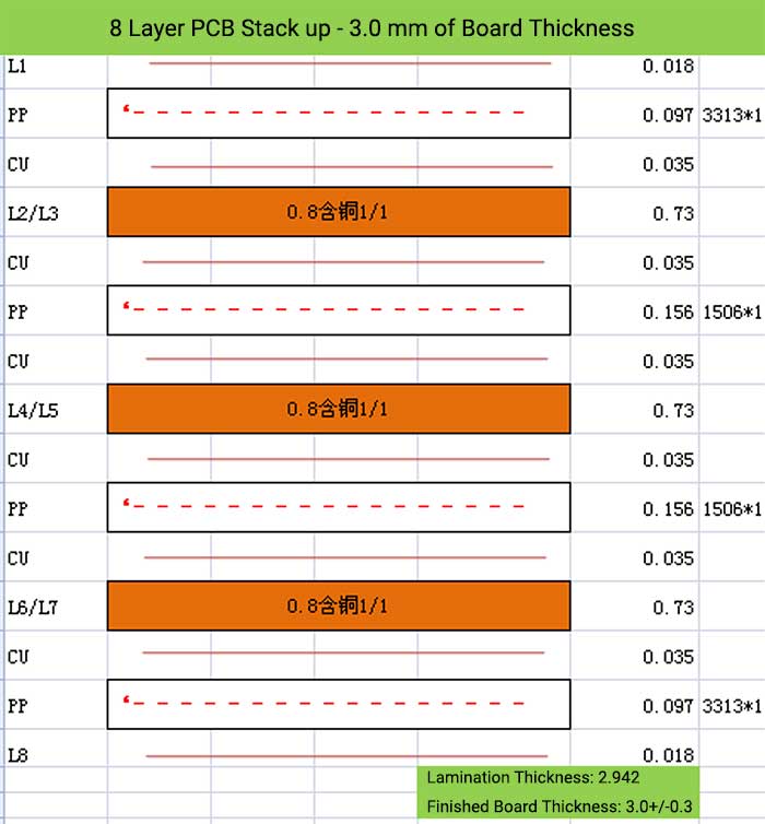
8 Layer PCB Stack up – 3.0 mm of Board Thickness

8 Layer PCB Stack up - 3.2 mm of Board Thickness

8 Layer PCB Stack up – 3.2 mm of Board Thickness

10 Layer PCB Stack up - 1.0 mm of Board Thickness

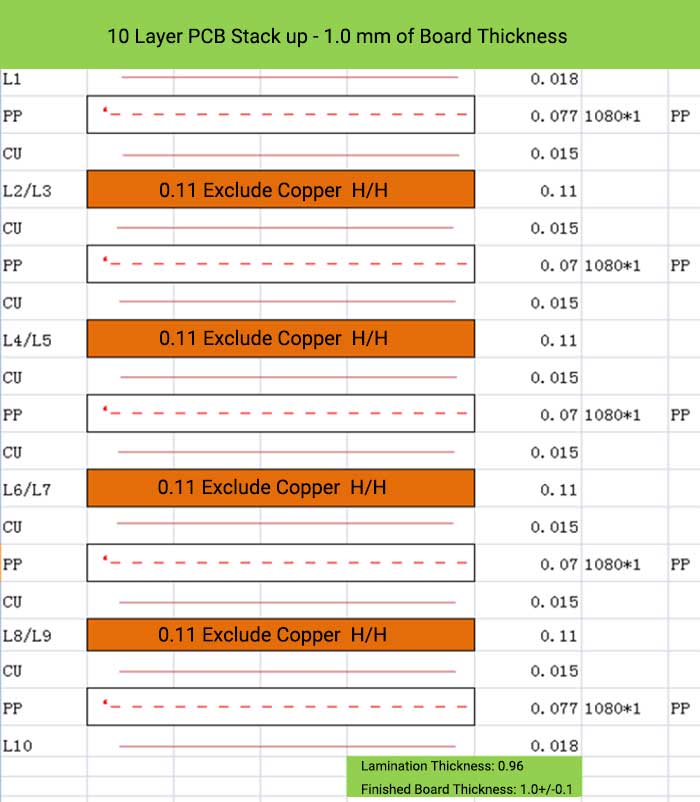
10 Layer PCB Stack up – 1.0 mm of Board Thickness

10 Layer PCB Stack up - 1.2 mm of Board Thickness

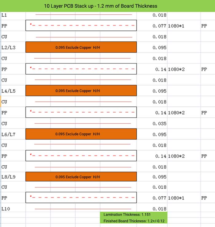
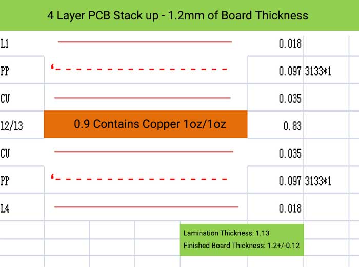
10 Layer PCB Stack up – 1.2 mm of Board Thickness

10 Layer PCB Stack up - 1.6 mm of Board Thickness

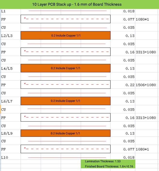
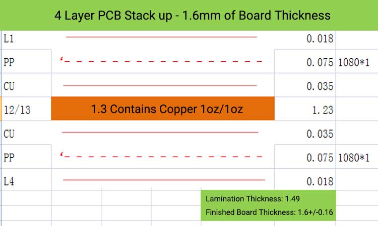
10 Layer PCB Stack up – 1.6 mm of Board Thickness

10 Layer PCB Stack up - 2.0 mm of Board Thickness

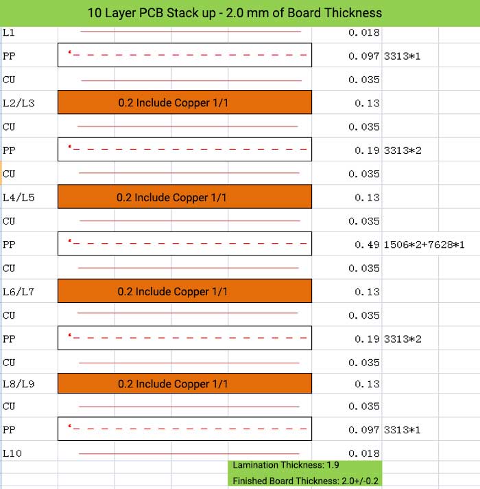
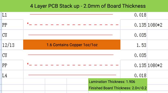
10 Layer PCB Stack up – 2.0 mm of Board Thickness

10 Layer PCB Stack up - 2.2 mm of Board Thickness

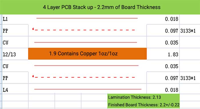
10 Layer PCB Stack up – 2.2 mm of Board Thickness

10 Layer PCB Stack up - 2.4 mm of Board Thickness

10 Layer PCB Stack up – 2.4 mm of Board Thickness

10 Layer PCB Stack up - 2.6 mm of Board Thickness

10 Layer PCB Stack up – 2.6 mm of Board Thickness

10 Layer PCB Stack up - 2.8 mm of Board Thickness

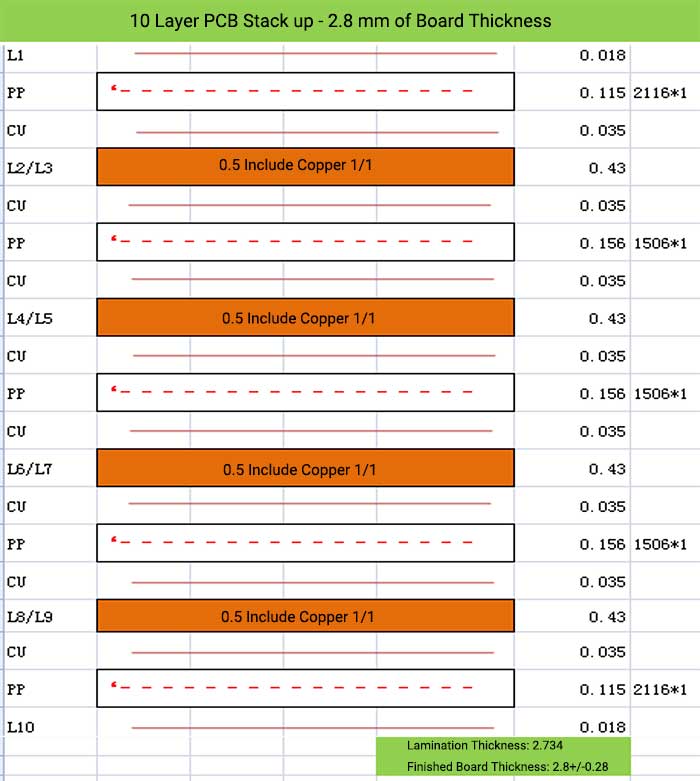
10 Layer PCB Stack up – 2.8 mm of Board Thickness

10 Layer PCB Stack up - 3.0 mm of Board Thickness

10 Layer PCB Stack up – 3.0 mm of Board Thickness

10 Layer PCB Stack up - 3.2 mm of Board Thickness

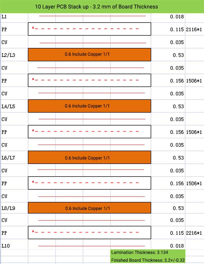
10 Layer PCB Stack up – 3.2 mm of Board Thickness

12 Layer PCB Stack up - 1.2 mm of Board Thickness

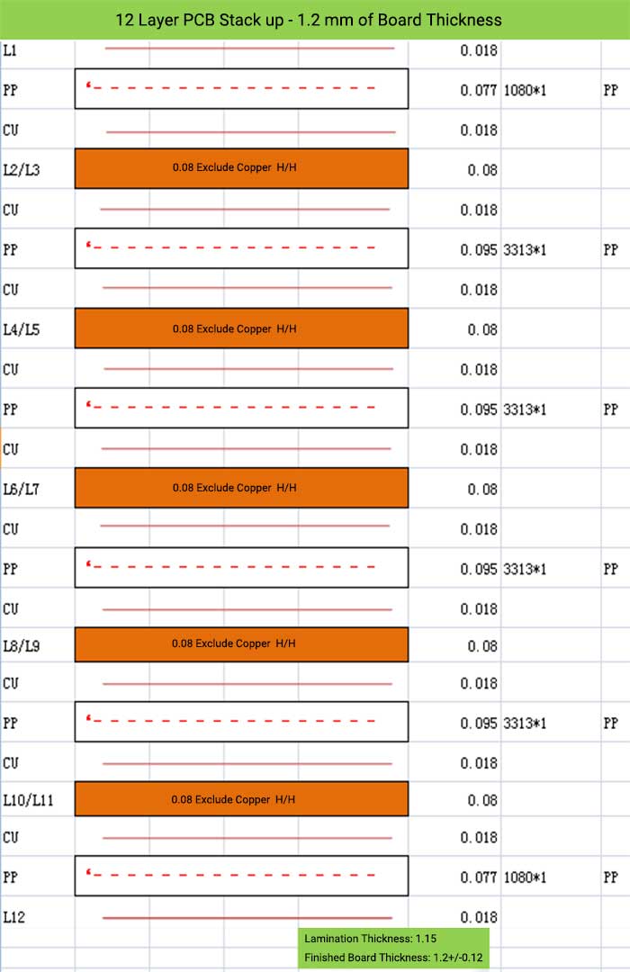
12 Layer PCB Stack up – 1.2 mm of Board Thickness

12 Layer PCB Stack up - 1.6 mm of Board Thickness

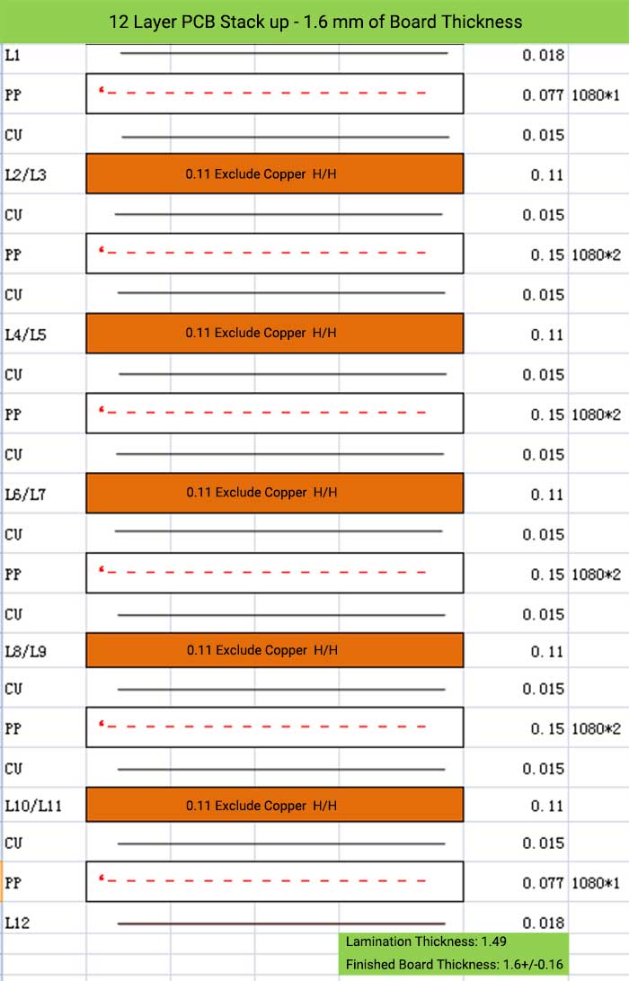
12 Layer PCB Stack up – 1.6 mm of Board Thickness

12 Layer PCB Stack up - 2.0 mm of Board Thickness

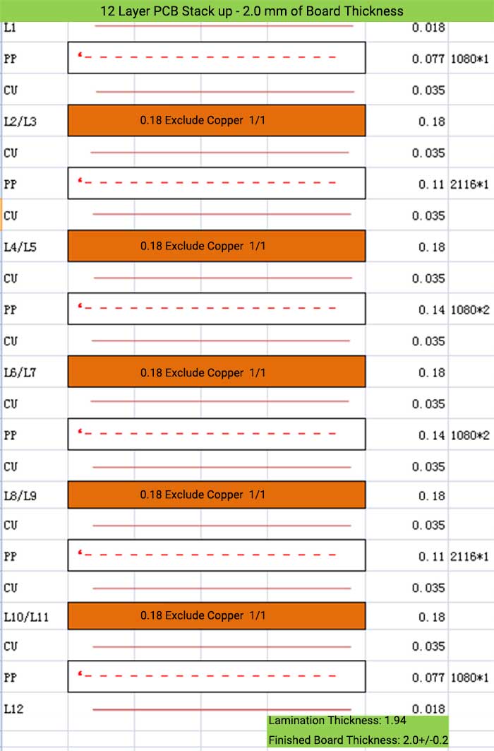
12 Layer PCB Stack up – 2.0 mm of Board Thickness

12 Layer PCB Stack up - 2.2 mm of Board Thickness

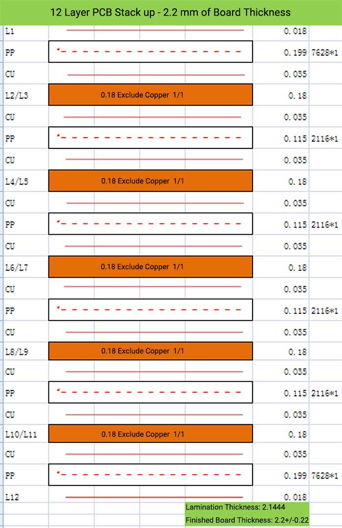
12 Layer PCB Stack up – 2.2 mm of Board Thickness

12 Layer PCB Stack up - 2.4 mm of Board Thickness

12 Layer PCB Stack up – 2.4 mm of Board Thickness

12 Layer PCB Stack up - 2.6 mm of Board Thickness

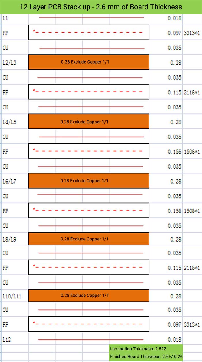
12 Layer PCB Stack up – 2.6 mm of Board Thickness

12 Layer PCB Stack up - 2.8 mm of Board Thickness

12 Layer PCB Stack up – 2.8 mm of Board Thickness

12 Layer PCB Stack up - 3.0 mm of Board Thickness

12 Layer PCB Stack up – 3.0 mm of Board Thickness

12 Layer PCB Stack up - 3.2 mm of Board Thickness

12 Layer PCB Stack up – 3.2 mm of Board Thickness

14 Layer PCB Stack up - 1.6 mm of Board Thickness

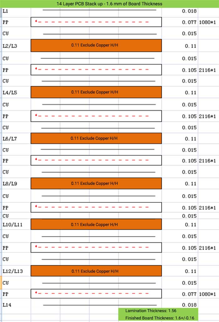
14 Layer PCB Stack up – 1.6 mm of Board Thickness

14 Layer PCB Stack up - 2.0 mm of Board Thickness

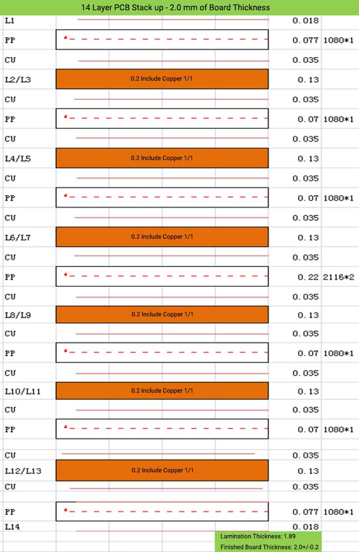
14 Layer PCB Stack up – 2.0 mm of Board Thickness

About Me

JHYPCB is a leading PCB prototyping, PCB manufacturing and assembly service provider in China, offering quick turn PCB prototyping, multi-layer PCB manufacturing and turnkey PCB assembly services.

Recent Posts

PCB assembly service
Scroll to Top