A flexible PCB coverlay is applied during the manufacturing process of flexible PCBs to enclose and protect the flexible PCB’s copper structure (external circuitry and wiring). It is a covering film that is made of a thick sheet of either acrylic or polyimide and a flexible adhesive layer that is laminated under high temperatures and then pressurized onto the surface of the circuit. The main function of a flexible PCB coverlay is to protect the base of the flexible printed circuit material. It has a high-temperature resistance which allows it to be used in heaters and ovens.
A flexible PCB coverlay provides the same functionality as a solder mask used on rigid PCBs. However, a flexible PCB coverlay offers more durability and flexibility which are very important in the application of flexible printed circuits compared to a solder mask with limited flexibility.
What is FPC Coverlay?
What Is A Flexible PCB?
Flexible PCBs, also known as Flexible Printed Circuits (FPC) or Flex PCBs, are an enhanced type of printed circuit board with the capability and flexibility to bend, fold, or twist into any desired shape. Initially, printed circuit boards were developed with solid base materials called substrates and, as a result, were available only in solid forms (board-shaped). With the advancement in technology and further research, scientists imagined PCBs that could bend easily and fit into desirable shapes. Thus, flexible PCBs were developed.
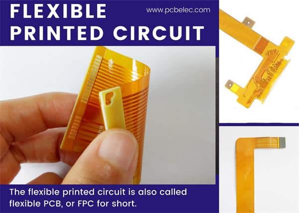
Flexible PCBs are an incredible addition to the electronic industry. They are light-weighted, flexible, and occupy less space. Flexible printed circuits have a wide range of applications in consumer appliances and wearable products, military, financial, medical, automotive, and telecommunications industries, and others.
Flexible PCBs are expensive and are usually designed by tech companies for end-users electronic products. Features of flexible PCBs include:
- Reduced space and weight
- Easily customized
- Conforms to specific flexing requirements like in mobile phones and other consumer electronic products
- Flexibility for easy installation and services like solar panels, satellites, and power generators.
- Impedance control
- Improved reliability and reproductivity
- Thermal management
- Eliminate the need for connectors
- Reduces cost of production and assembly of components
- Improve aesthetics
- Increase scalability and expansibility which enable several components to be interconnected on a circuit board to design a larger device
- Offers uniform electrical features for high-speed electric circuits
- Improve signal quality and integrity by minimizing noise reflection.
What Is Flexible PCB Coverlay?
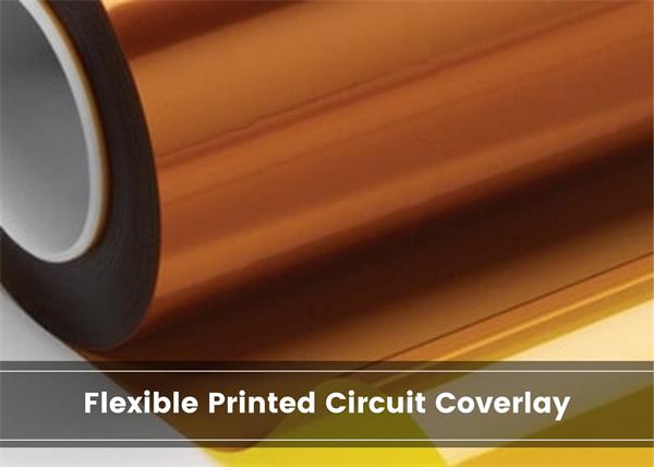
Flexible PCB coverlay’s major function is to protect the circuitry on the flexible PCB. It acts as the solder resist or solder mask for flexible printed circuit boards. Conventional solder masks or solder resist having limited ductility or flexibility. So for flexible printed circuits that need greater flexibility, flexible PCB coverlay is affixed on the circuit board for the protection of the copper foils and wirings. Flexible PCB coverlay is frequently used and the most preferred solution for enclosing layers of the external circuit of a flexible printed circuit in the PCB industry. It provides a more durable and robust solution with excellent flexibility and high dielectric strength.
Flexible PCB Coverlay is a solid sheet of material with two parts comprising of one layer of either acrylic or epoxy-based flexible adhesives and one layer of polyimide. The adhesive bonds the polyimide into the flexible circuit and enclosed the circuitry. The flexible PCB coverlay is then aligned to the surface of the circuit and aligned under specific temperature and pressure.
Flexible PCB coverlay exists in various combinations of the thickness of the adhesive and film. The most frequently used combination is in ratio 1:1 (that is 1 mil film and 1 mil adhesive). The specific combination of the films and adhesives is dependent on these items below:
- Minimum bending requirements. Thinner coverlay might be needed to meet tougher bending requirements
- The weight of the external copper layers
- Dielectric resistance voltage (in some cases)
- Cost
The natural brown coloration of a flexible PCB coverlay is frequently seen when you take a look at a flexible printed circuit. Since coverlay is a solid sheet of polyimide, it has similar dielectric voltage resistance as flexible cores of polyimide-approximately 3KV per 0.001 inch-and it is available in various thicknesses for various bending requirements.
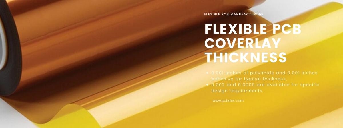
What Is The Thickness of Flexible PCB Coverlay?
The thickness of a typical flexible PCB coverlay is 0.001 inches of polyimide and 0.001 inches adhesive. A thickness of 0.002 and 0.0005 is available and only used when necessary to meet certain design requirements.
What Is The Difference Between Flexible PCB Coverlay And Solder Mask Layer?
The circuitry of the exposed external layers of flexible printed circuits can be encapsulated with either a polyimide coverlay or a flexible solder resist or solder mask. Although both materials perform the same primary function of protecting or insulating the circuitry of the outer layer of a flexible PCB, each material has different features, capabilities, and characteristics that are suitable for certain particular design requirements.
The differences between flexible PCB coverlay and solder mask are:
- A flexible PCB coverlay is a combination of adhesive and Kapton (a polyimide) but a solder mask (solder resist) is liquid-based.
- Coverlay dam sizes should be kept at 10 mils minimum; however, solder mask dam sizes should be kept at 4 mils minimum. The dam stops the flowing of molten, liquefied solder from one pad to another pad nearby
- The trace to mask opening for coverlay can be as close as 3 mils. However, using 3 mils for solder masks could cause undercut or non-recording issues (with respect to the imaging of solder masks). It is advisable you maintain a minimum distance of 4 mils for a solder mask.
- Coverlay is generally used on the flexible sections of flexible printed circuits. A solder mask is made use of on the hard or rigid section of the PCB. However, if you want to make use of coverlay on an entire rigid-flexible PCB, ensure fang opening or window opening is present.
- Unlike a solder mask, coverlay cannot be used on pitch components.
Conclusion
Flexible PCB Coverlay offers effective protection and insulation to the circuitry of external layers of a flexible PCB which addresses various design requirements. It is also important you understand the differences between a coverlay and a solder mask to facilitate your flexible PCB designs.
Related Reading
- A Complete Guide To Single-Sided Flex Circuits
- A Completed Guide Of Double-Sided Flexible PCB
- Everything You Need To Know About Multilayer Flexible PCB
- What is Flexible PCB Prototype?
- What Are Flexible PCB Stiffeners?
- Rigid PCB vs Flex PCB: What Is The Difference?
- The Manufacturing Process Of Double-sided Flexible PCB Coverlay
- Custom Flex PCB:Tailored Solutions for Your Applications
- Finding the Right China PCB Manufacturers:5 Vetting Tips
- Introduction to Semi-Flex PCBs: Bridging Rigid and Flex PCBs
- Flexible PCB Manufacturing: A Guide to Fabrication and Assembly
- Flexible PCB MaHow to Select the Right Flexible PCB Manufacturer for Your Product: A 6-Step Guidenufacturing: A Guide to Fabrication and Assembly
- What Are The Types of Flexible Circuit Boards?
- Top Applications of Flexible Printed Circuit Boards in 2024
- What Are The Advantages And Applications Of Rigid-Flex PCBs?


