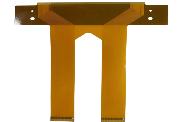
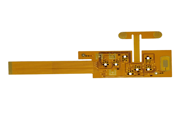
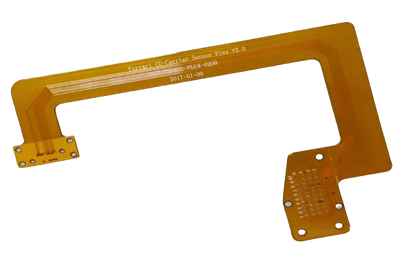
Generally, a PCB made of a flexible insulating substrate is called a flexible PCB or FPC, and a circuit board that combines a rigid PCB and a flexible PCB is called a rigid-flex PCB. It meets the needs of today’s electronic products in the direction of high density and high reliability, miniaturization, and lightweight. It also meets the strict economic requirements and the needs of market and technology competition.
1. Basic knowledge of flexible circuit board
Flexible PCBs are usually classified as follows according to the number of layers and structure of conductors:
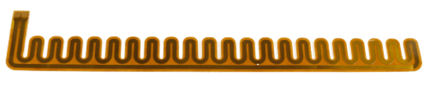
1.1 single-sided Flexible PCB
Single-sided flexible PCB has only one layer of conductor, and the surface can be covered or not.
The insulating base material used varies with the application of the product.
Commonly used insulating materials are polyester, polyimide, polytetrafluoroethylene, and soft epoxy-glass cloth.
Single-sided flexible PCBs can be further divided into the following four categories:
1) Flexible circuit board with single side connection without covering layer
The conductor pattern of this kind of flexible PCB is on the insulating substrate, and the conductor surface has no covering layer—it like a standard single-sided rigid PCB.
This type of product is the cheapest one, usually used in non-critical and environmentally friendly applications.
The interconnection is realized by soldering, welding, or pressure welding.
It is often used in early telephones.
2) Flexible circuit board with cover layer connected on one side
Compared with the previous type, this type only has an extra layer of coverage on the surface of the wire according to customer requirements.
The pads need to be exposed when covering.
If precision is required, the form of a clearance hole can be adopted.
It is the most widely used single-sided flexible PCB and is commonly used in automotive instruments and electronic instruments.
3) Flexible circuit board with a double-sided connection without covering layer
This type of connection pad interface can be connected to the front and back of the wire.
To this end, a via hole is opened on the insulating substrate at the pad. The via hole can be punched, etched, or made by other mechanical methods at the required position of the insulating substrate.
It is used to mount components and devices on both sides and where soldering is required. There is no insulating substrate in the pad area of the via. Chemical methods usually remove such a pad area.
4) FPC with cover layer connected on both sides
This type of FPC has a covering layer on the surface. However, the cover layer has via holes, which allow termination on both sides and still maintain the cover layer.
This kind of flexible PCB comprises two layers of insulating materials and a layer of metal conductors.
It is used on occasions where the covering layer and the surrounding devices need to be insulated from each other, and the ends need to be connected to both the front and back sides.
1.2 Double-sided Flexible PCB
Double-sided flexible PCB with two layers of conductors.
The application and advantages of this type of double-sided flexible PCB are the same as those of a single-sided flexible PCB. Its main advantage is to increase the wiring density per unit area.
It can be divided into with or without metalized holes and with or without covering layer:
- Without metalized holes, without covering layer;
- Without metallization holes and covering layers;
- With metalized holes and no covering layer;
- With metalized holes and covering layer.
The double-sided flexible PCB without the covering layer is rarely used.
1.3 Multilayer Flexible PCB
Flexible multilayer PCB adopts multilayer lamination technology like rigid multilayer PCB to make multilayer flexible PCB.
The simplest multilayer flexible PCB is a three-layer flexible PCB formed by covering two copper shielding layers on both sides of a single-sided PCB.
This three-layer flexible PCB is equivalent to a coaxial wire or a shielded wire in electrical characteristics.
The most commonly used multilayer flexible PCB structure is a four-layer structure, which uses metalized holes to realize inter-layer interconnection. The middle two layers are generally the power layer and the ground layer.
The advantage of multilayer flexible PCB is that the base film is light in weight and has excellent electrical properties, such as low dielectric constant. The multilayer flexible PCB board is made of polyimide film as the base material is about 1/3 lighter than the rigid epoxy glass cloth multilayer PCB board. Still, it loses the excellent single-sided and double-sided flexible PCB. Most of these products do not require flexibility.
2. Flexible printed circuit board plating
(1) Pretreatment of FPC plating
The surface of the copper conductor exposed by the flexible printed board after the coating process may be contaminated by adhesive or ink. There may also be oxidation and discoloration due to the high-temperature process. To obtain a dense coating with excellent adhesion, the conductor must be The pollution and oxide layer on the surface are removed to make the surface of the conductor clean. However, some of these pollutions are very strong in combination with copper conductors and cannot be eliminated with weak cleaning agents. Therefore, most of them are often treated with a particular strength of alkaline abrasives and brushing. The covering adhesives are mostly rung. Oxygen resin has weak alkali resistance, which will lead to a decrease in bonding strength. Although it will not be visible, in the FPC plating process, the plating solution may penetrate from the edge of the cover layer, and the cover layer will peel off in severe cases. In the final welding, the solder penetrates under the covering layer. It can be said that the pre-treatment cleaning process will have a significant impact on the essential characteristics of the flexible printed circuit board FPC, and full attention must be paid to the processing conditions.
(2) The thickness of FPC plating
During electroplating, the deposition speed of the electroplated metal is directly related to the electric field intensity, and the electric field intensity changes with the shape of the circuit pattern and the positional relationship of the electrodes. Generally, the thinner the wire width, the sharper the terminal of the terminal part, the closer the distance to the electrode, the higher the electric field strength, and the thicker the plating layer at this part.
(3) The stains and dirt of FPC plating
The state of the plating layer that has just been electroplated, especially the appearance, is not a problem. But, soon, some surfaces have stains, dirt, discoloration, etc., especially when the factory inspection did not find anything unusual. Still, when the user conducts an acceptance inspection, it Found that there is an appearance problem. This is caused by insufficient drifting and residual plating solution on the surface of the plating layer, which is caused by the slow chemical reaction over some time. Especially flexible printed boards, because they are soft and not very flat, various solutions are prone to “accumulate?” in the recesses and then react and change color in this part. To prevent this from happening, it must be entirely drifted and necessary to perform sufficient drying treatment. The high-temperature thermal aging test can be used to confirm whether the drift is adequate.
3. Chemical plating of flexible PCB
When the line conductor to be plated is isolated and cannot be used as an electrode, only electroless plating can be performed. Generally, the plating solution used in electroless plating has a definite chemical effect, and the electroless gold plating process is a typical example. The electroless gold plating solution is an alkaline aqueous solution with a very high pH. When using this kind of electroplating process, it is easy for the plating solution to drill under the covering layer, especially if the quality control of the covering film lamination process is not strict and the bonding strength is low; this problem is more likely to occur.
Due to the characteristics of the plating solution, the electroless plating of displacement reaction is more prone to the phenomenon that the plating solution penetrates under the covering layer, and it is challenging to obtain ideal plating conditions with this process.
4. Hot air leveling of FPC
The hot air straightening of the plain was initially developed to coat the rigid PCB with lead and tin. Because this technology is simple, it has also been applied to the flexible printed circuit board. Hot air leveling is to immerse the board in a molten lead-tin bath directly and vertically and blow off the excess solder with hot air. This condition is very harsh for the flexible PCB. If the FPC cannot be immersed in the solder without any measures, the FPC must be clamped between the screen made of titanium steel And then dipped in molten solder; of course, the surface of the flexible PCB must be cleaned and coated with flux in advance.
Due to the harsh conditions of the hot air leveling process, it is easy to cause the solder to drill from the end of the cover layer to under the cover layer. This phenomenon is more likely to occur frequently when the bonding strength between the cover layer and the copper foil surface is low. Since polyimide film is easy to absorb moisture, when the hot air leveling process is used, the moisture absorbed will cause the cover layer to bubble or even peel off due to the rapid heat evaporation. Therefore, before the FPC hot air leveling, it must be dried and moisture-proof management.
Advanced Learning:


