sales@pcbjhy.com

Sales Manager: Ms. Megan

+86-13825274100

24/7 Customer Support

+86-13825274100

WeChat and WhatsApp

What is the Difference Between PTH and Via in PCBs?

Understanding the key differences between PTH and via is essential for optimizing PCB design and manufacturing. This article defines PTH and via, compares dimensions, functions, locations and finishing requirements. Typical applications and design considerations are also discussed.
What is the Difference Between PTH and Via in PCBs?

Table of Contents

Demystifying the Critical Differences: PTH vs. Via in PCB Design

PCBs serve as the foundation for almost all modern electronics. They provide the mechanical structure and electrical connections between components. In order to facilitate these electrical connections, PCBs utilize plated through holes (PTHs) and vias. Both PTHs and vias enable conduction between different layers in multilayer PCB designs. However, confusing these terms can lead to suboptimal PCB design and manufacturing defects.

As PCB technology continues advancing into higher densities and more complex multilayer designs, understanding the differences between PTHs and vias becomes increasingly important. This article will clearly define PTHs and vias, compare their key characteristics, describe their typical applications, and provide design considerations when utilizing them. Grasping these distinctions will equip PCB designers and manufacturers to optimize their products.

Via Types in PCB Board

Defining PTH and Vias in PCBs

Before diving into how PTHs and vias differ, it is important to accurately define each term.

PTHs: PTHs are vertical holes that span entire multilayer PCBs and enables conduction between layers. The holes typically have a diameter between 0.15mm to 2mm. The walls of the holes are plated with copper to facilitate electrical connectivity. PTHs primarily function to connect surface mount pads or through hole pads to internal traces and planes. This enables mounting and interconnecting electronic components.

Vias: Vias are also vertical interconnects but they are localized connections within or between layers of a PCB. Vias have smaller diameters than PTHs, usually between 0.1mm to 0.5mm. While PTHs function mainly for component connections, vias are primarily used to route signals between traces on different layers. Their purposes focus more on allowing trace routing rather than component placement.

PTH vs Via - Contrasting Dimensions, Locations and Functions

While PTHs and vias share some high-level similarities as vertical interconnects in multilayer PCBs, they have distinct differences:

Locations: The most fundamental difference is PTHs span entirely through boards, while vias only connect within or between layers. PTHs make connections through the whole PCB stackup. Vias link traces in planar sections.

Functions: Due to their placement, PTHs primarily enable mounting and connecting components. The through hole pads provide anchoring points for leads to be soldered. Vias mainly function to reroute signals between layers when optimal trace routing is unavailable on the same plane.

Dimensions: PTHs require larger diameters to accommodate component leads, generally ranging from 0.15mm to 2mm. Vias only need to link thin traces, so appropriately have smaller diameters between 0.1mm to 0.5mm. Narrower dimensions allow higher via densities.

Finishing: For soldering components, PTHs often require solder masking over pads and special hole preparations. Vias do not undergo soldering so lack finishing requirements. No solder masking or hole preparations are involved.

PTH vs. Via - Key Characteristic Comparison

Plated Through Hole (PTH) Via
Definition A hole with copper plating An electrical connection between layers
Purpose Provides electrical connection between layers or to components Establishes electrical connections between layers
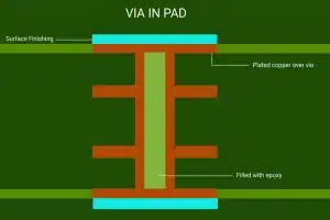
Construction Copper plating extends through the entire hole Copper pad connects the layers through the hole
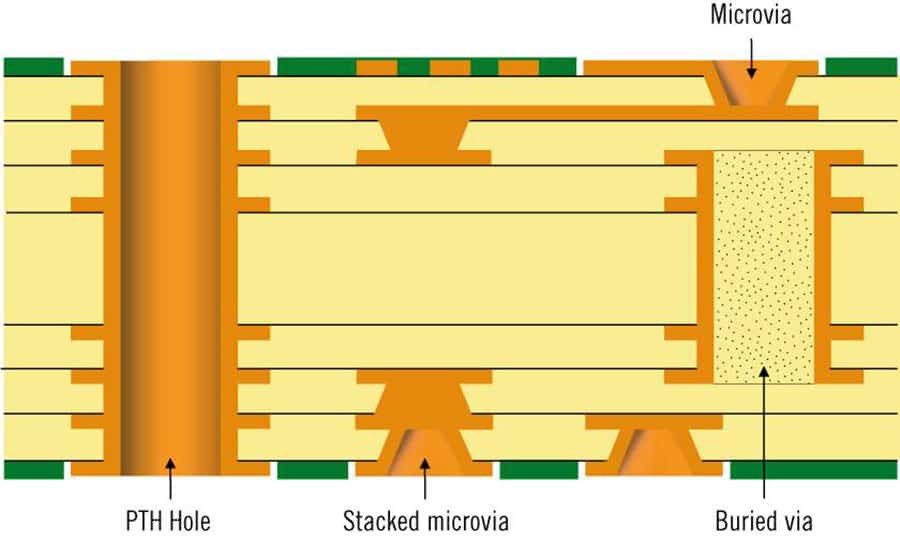
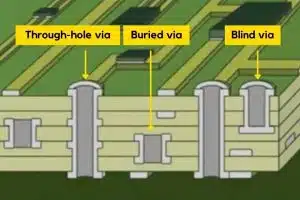
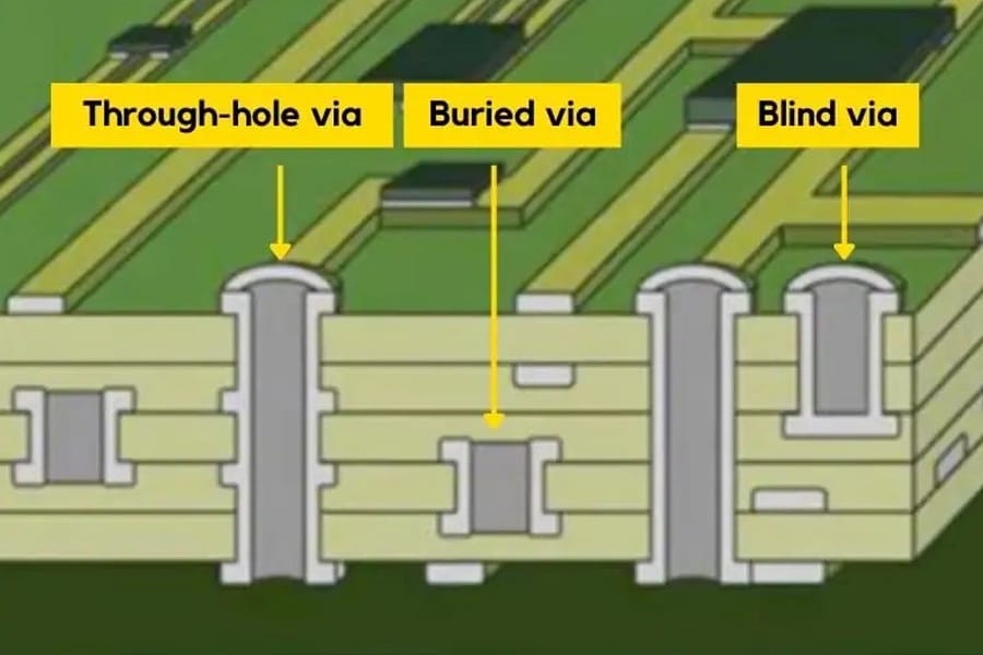
Types Single-sided, double-sided, and multilayer PTH Through-hole via, blind via, buried via
Component Mounting Components can be mounted directly into PTHs Components are not mounted directly into vias
Conductivity High conductivity due to complete copper plating Conductivity depends on the plating and inner layer connections
Size Larger in diameter to accommodate components Smaller in diameter for signal routing
Application Suitable for components requiring a strong mechanical connection Used for interconnecting signal and power traces

Real-World Usages: When to Use PTHs and When to Use Vias

Because PTHs and vias serve distinct interconnect purposes in PCBs, they consequently have unique applications:

PTH Applications:

  1. Component lead connections – PTHs allow leads from through-hole components to pass through the entire board and be soldered for both mechanical anchoring and electrical conductivity.
  2. Multi-layer stacking – The spanning nature of PTHs enables connectivity across entire multi-layer PCB stackups, ideal for high-density designs.
  3. Power planes – The larger dimensions of PTHs is suited for connections to thicker power and ground planes spread across layers.
  4. Shielding – Grounded PTHs positioned around components or board areas provide shielding from EMI and crosstalk.

Via Applications:

  1. Escape routing – When surface traces are congested, vias allow the routing to change layers to escape routing difficulties.
  2. Layer translation – Vias transition signals between layers when ideal trace paths span separate PCB layers.
  3. Component pads – Occasionally vias integrate into surface mount pads for heat dissipation drainage.
  4. Stitching – Multiple vias can stitch together areas on layers needing greater conductivity.

PTH and Via Design Guidelines for Optimal PCB Fabrication

When leveraging PTHs and vias in a PCB layout, designers should keep the following guidelines in mind:

For PTHs:

  • Match hole diameters to leads – Ensure clearances between component leads and PTH walls are neither oversized nor too constrained to avoid issues like backdrainage or poor hole filling.
  • Mind padstack impacts – An excessive number of PTH padstacks can burden manufacturing processes. Optimizing quantity and layout benefits fabrication yield.
  • Accommodate thermal reliefs – Allow sufficient thermal reliefs for high power PTH connections to prevent solder joint or plated copper damage.

For Vias:

  • Check minimum annular rings – Verify vias meet annular ring requirements for reliable plating quality and solder resist coverage.
  • Consider signal impedance – Excessive or tightly spaced vias can negatively impact signals like high-speed data lines. Balance layout carefully.
  • Ensure filled vias cannot trap moisture – Blind and buried vias especially need proper filling to avoid popped solder joints from moisture expansion.

Key Takeaways - Why Understanding PTHs vs Vias Matters

In summary, PTHs and vias both enable vertical conductivity through a PCB, but have distinct differences:

  • PTHs span entire multilayer boards while vias only interconnect locally within or between adjacent layers
  • PTHs connect components across layers whereas vias route traces between layers
  • PTHs require larger diameters to accommodate leads whereas vias only need minor trace-sized holes
  • PTHs involve padstack finishing for soldering while vias lack holes preparations

Properly differentiating between PTHs and vias is imperative for optimizing PCB design and manufacturing. Misapplication can lead to increased fabrication difficulties and degraded product performance. By correctly leveraging PTHs and vias for their intended purposes, circuit designers can maximize available space, routing efficiencies, and signal integrity. Keeping these interconnects properly separated ultimately allows creating smaller, faster, cheaper, and more reliable electronics.

Related Posts

About Me

JHYPCB is a leading PCB prototyping, PCB manufacturing and assembly service provider in China, offering quick turn PCB prototyping, multi-layer PCB manufacturing and turnkey PCB assembly services.

Recent Posts

PCB assembly service
Scroll to Top