Flexible Circuit Boards: The Future of Compact Electronics
As electronics get increasingly compact and integrated into tighter spaces, the need for flexible printed circuit boards (flex PCBs or flexible PCBs) has skyrocketed. Unlike traditional rigid PCB boards, these unique circuits offer unmatched flexibility, reliability, and space savings.
Flex PCBs consist of flexible base materials like polyimide laminated with copper conductor layers. Unlike rigid PCBs, they can be bent, twisted, or folded without compromising functionality. This exceptional flexibility allows flex circuits to adapt to 3D shapes and fit into confined spaces where rigid boards cannot.
The core advantages of flexible circuit boards include:
- Space Optimization: Their thin, bendable nature enables ultra-compact designs and efficient use of available space.
- Weight Reduction: Significantly lighter than rigid PCBs with reduced connectors and cabling.
- Reliability: Increased resistance to vibration, temperature fluctuations, and physical stress.
- Design Versatility: Can conform to virtually any shape for creative product designs.
From wearable technology to aerospace systems, the applications of flexible PCBs span numerous industries. As miniaturization trends accelerate, these flexible marvels will continue to unlock new possibilities for innovative electronics.
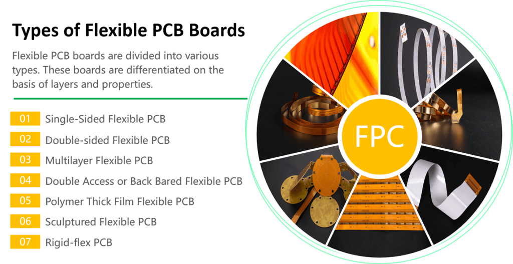
Types of Flexible Circuit Boards Explained
Single sided Flexible PCB
This is the simplest flexible PCB type with only one conductive layer. A thin flexible dielectric film, such as Polyimide, is used. There is only one conductive layer on the board.
Single-sided flex circuits are the simplest and most economical option among the various flex PCB types. As the name suggests, these flexible PCBs feature just one conductive copper layer laminated on one side of the flexible dielectric substrate, typically polyimide.
The single copper layer design of flexible single-sided PCBs makes them ideal for basic, low-density circuit applications where flexibility and low costs are priorities. Some key advantages of single-sided flexible circuit boards include:
- Cost-effectiveness for simple, flexible PCB needs
- Excellent flex life and dynamic flex capabilities
- Compact, lightweight construction
- Suitable for various flex radii and complex 3D shapes
Common applications that benefit from single-sided flexible PCBs include wearable technology, bendable electronic displays, portable medical devices, and other products requiring flexible form factors.
While offering unmatched convenience and flexibility, single-layer flex PCBs are best suited for straightforward, low-complexity circuit designs. Multi-layer flexible circuit board options provide higher wiring densities for more advanced requirements.
Double Sided Flexible PCBs - More Routing Density
Double-sided flexible PCBs have two conductive layers, one on each surface. You have components or conductive lines on both sides. These flexible circuits are more economical compared to single-sided flexible PCBs.
Stepping up from single-sided flex circuits, double-sided flexible PCBs feature copper conductive layers on both sides of the flexible base material. This Construction allows for dramatically increased wiring density and routing capabilities compared to single-layer flexible boards.
The key advantages of double-sided flexible printed circuit boards include:
- Higher component packaging density with components on both sides
- Complex, high-density interconnect routing possible
- Increased functionality integration in a compact footprint
- Cost-effective alternative to multi-layer flex for mid-complexity designs
Double-sided or “dual access” flexible circuits strike a balance between the basic single-layer flex PCBs and advanced multilayer flexible boards. Their enhanced routing space accommodates moderately complex circuits and electronic functionality.
These double-layer flex PCBs find wide use across industries like:
- Medical devices requiring portability and flex characteristics
- Wearable technology relying on compact, conformable form factors
- Aerospace and military applications needing rugged flex capabilities
While more costly than single-sided flexibles, double-sided or dual-access flexible printed circuit boards offer a versatile solution for intricate yet cost-sensitive designs requiring dynamic bending and flex characteristics.
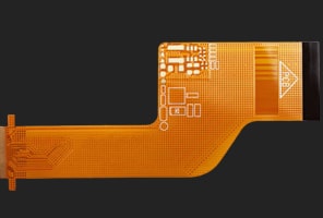
Multilayer Flexible PCBs - Ultimate Routing Density
In a multilayer flexible PCB, there are multiple conductive layers of copper. It has at least three copper/conductive layers or more. There is a thin layer of PI between two conductive layers. These layers are interconnected with the help of vias.
Multilayer flexible printed circuit boards provide the ideal solution for applications demanding extremely high wiring and circuit densities combined with dynamic flex performance. These advanced flex circuits contain three or more layers of copper conductor laminates separated by thin flexible dielectric films.
Key advantages of multilayer flexible circuit boards include:
- Unmatched high-density wiring and component packaging capabilities
- Support for highly integrated and complex electronic functionalities
- Increased signal integrity and power/ground plane versatility
- Exceptional flex life and ability to form complex 3D shapes
The layered construction of multilayer flex PCBs enables stacking of intricate circuitry and interconnects within a compact footprint that can bend, fold, and twist as needed. This makes them ideal for demanding applications across sectors like:
- Aerospace/Defense systems requiring ruggedness and reliability
- Compact, feature-rich portable medical/instrumentation devices
- High-performance automotive and industrial electronics
While multilayer flexible printed circuit boards involve higher fabrication costs, their unparalleled flexibility and high-density capabilities justify the investment for cutting-edge products where performance and reliability are paramount.
Double Access/Back Bared Flexible PCBs - Dual-Sided Value
Dual access or back bare flexible PCB is a particular type of single-sided flexible circuit. There is only one layer of copper, but it is arranged in a special manner to be accessed from both sides. This is the specialty of a dual-access flexible circuit.
Double access or back-bared flex PCBs offer a unique, cost-effective solution among the various flexible printed circuit board types. Despite having only a single conductive layer, these flexible circuits utilize a specialized manufacturing process to expose the copper traces on both sides.
This innovative “back baring” design provides some key advantages:
- Cost savings vs. double-sided flex PCBs with two copper layers
- Allows component mounting and probe-test access on both sides
- Retains flexibility and 3D formability of single-layer flex circuits
- Enables moderately complex, double-access circuit routing
Back-bared or double-access flexible PCBs strike the perfect balance for applications requiring dual-sided functionality at lower costs than true double-sided flex. Some common uses include:
- Cost-sensitive consumer electronics like wearables and IoT devices
- Compact, disposable medical sensors and diagnostic equipment
- Simple industrial controls and instrumentation
While lacking the high-density capabilities of multilayer flexible printed circuit boards, double access back bared flexes provide ample routing and functionality for many cost-constrained designs benefitting from dual-sided access and flexibility.
Polymer Thick Film Flexible PCBs - Printed Circuitry
Polymer Thick Film (PTF) flexible circuits are real printed circuits. Several types of conductive inks are used to print the circuit on the base. Most of the time, the ink is applied with the help of stencils. Most of the time, the ink is applied with the help of stencils.
Polymer thick film flexible printed circuit boards take a unique manufacturing approach compared to traditional flex PCBs. Instead of using copper laminates, the conductive circuitry is printed directly onto the flexible substrate using specialized conductive polymer inks.
This printed electronics process offers some distinct advantages:
- Enables extremely fine line widths and trace geometries
- Supports truly 3D circuit layouts on curved surface profiles
- More eco-friendly fabrication without harsh etchants
- Potential for lower costs than traditional flex PCB fabrication
The printed conductive polymer circuits can be formed directly onto flexible base materials like polyimide or polyester films. This allows polymer thick film flexibles to conform to virtually any 3D shape or dynamic flex requirements.
While typically having lower overall circuit density than copper-based flex PCBs, polymer thick film technology finds use in many innovative applications:
- Flexible displays and curved sensor arrays
- Wearable electronics and e-textiles
- Disposable/single-use medical device sensors
- Specialized industrial and IoT sensor nodes
As printed electronics capabilities continue advancing, polymer thick film flexible printed circuit boards provide a unique blend of form factor flexibility with reduced environmental impact.
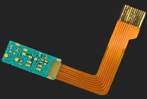
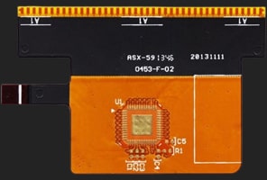
Rigid-Flex PCBs - Seamless Integration of Flex and Rigid
A rigid-flex PCB is a combination of rigid PCBs and flexible PCBs. There can be multiple rigid and flexible parts to create one circuit. The flexible part can bend easily, and the rigid part takes up the required space. Usually, the rigid parts are connected via flexible circuits.
Rigid-flex printed circuit boards represent the best of both worlds by integrating rigid and flexible circuits into a single seamless design. These hybrid constructions start as flexible circuit board laminates that are selectively reinforced during fabrication to create rigid PCB sections.
The unique rigid-flex architecture provides several key advantages:
- Combines reliable rigid areas for component mounting with flexible regions
- Eliminates connectors/cables between rigid and flex portions
- Enables complex 3D spatial routing and packaging density
- Reduces overall weight, space requirements, and potential failure points
Rigid-flex PCBs offer tremendous versatility for compact, lightweight applications requiring dynamic flexing and rigid integrated functionality. Some typical uses include:
- Aerospace avionics and controls
- Portable military/defense electronics
- Automotive engine/body control modules
- Robotics, industrial automation equipment
- Intensive mobile/handheld computing devices
While complex rigid-flex printed circuit boards involve higher fabrication costs, their compact integration of flex and rigid capabilities unlocks pioneering designs unmatched by separate rigid boards and flexes.
Advanced rigid-flex solutions continue pushing the boundaries for cutting-edge electronics across industries where size, weight, and reliability are paramount.
Flexible PCB Manufacturing Processes and Materials
The unique properties of flexible printed circuit boards stem from their specialized materials and manufacturing techniques. While differing in construction details, most flex PCB types share some common processes and materials.
Base Materials The core base material for flexible circuits is typically a polyimide film, chosen for its excellent thermal stability, chemical resistance, and flexibility. Other polymers like polyester or polyethylene naphthalate may also be used.
Copper Lamination Most flex PCBs use an adhesive layer to incorporate copper foil conductors laminated onto the base film. The copper foil thickness can range from very thin (9μm) to standard thicknesses seen in rigid PCBs.
Specialized adhesives and lamination processes ensure reliable copper-polymer bonding while maintaining flexibility. Common lamination methods include:
- Rolled lamination
- Vacuum lamination
- thermocompression bonding
Circuitry Formation For traditional copper-based flex PCBs, the Circuit traces are formed by imaging and etching the copper layer in much the same way as rigid PCBs.
Alternatively, polymer thick film (PTF) construction prints conductive metal-particle inks directly onto the base film using stencils or additive processes to form the circuit patterns.
Supporting Processes
Flexible circuits may undergo additional processes like:
- Laser depanelization/cutting
- Via formation and plating
- Component assembly (SMT, wire bonding, etc.)
- Conformal coatings
- Encapsulation and packaging
Rigid-Flex Fabrication For rigid-flex PCBs, portions of the flex laminate are selectively reinforced with stiffener materials like epoxy or metal plates during lamination to create rigid board areas integrated with flexible regions.
This advanced manufacturing enables the combined capabilities of both flexible and rigid printed circuit boards in a seamless geometry.
The inherent flexibility of the polymeric materials combined with specialized fabrication techniques empowers flexible PCBs to meet the demanding form factors of modern electronic products.
FAQs
Flexible printed circuit boards offer several advantages, including increased reliability, weight reduction, 3D packaging versatility, and the ability to fit into tight spaces that rigid boards cannot. Their dynamic flex and bend capabilities make them ideal for compact, portable electronics.
The base substrate is typically a flexible polymer film like polyimide, polyester or polyethylene naphthalate. The conductive circuitry is formed by laminating/bonding copper foil or printing with conductive inks.
When properly designed and manufactured, flexible circuits demonstrate excellent flex life and reliability. They can withstand substantial bending, twisting, and vibrations better than rigid PCBs. Protective coatings further enhance durability.
Single-layer flex PCBs have one conductive layer, double-layer flexible circuit boards have two copper layers on opposite sides, while multi-layer flex PCBs have three or more conductive layers laminated together, providing higher densities.
For simpler single/double-layer designs, flex PCBs can be very cost-effective. Multi-layer and rigid-flex PCB constructions do involve higher fabrication costs due to their complexity.
Flex PCB usage spans many sectors – consumer electronics, aerospace, military, medical devices, automotive, wearables and more. Any application benefits from lightweight, dynamic flexing, and compact packaging.
As a leading flexible PCB manufacturer in China, with over 10 years of experience in PCB manufacturing and assembly, alongside the latest technology and innovations at our fingertips to ensure we are providing the best quality products, we can offer the insights and advice to ensure you are making the right decision. If you have a product in mind and would like to discuss flexible PCBs in more detail, feel free to pick up the phone and speak to one of our friendly team or submit a quote.
Related Posts
- Custom Flex PCB:Tailored Solutions for Your Applications
- Custom PCB Fabrication in China – Prototyping & Mass Production
- Expedited PCB Services – Quick Turnaround for Your Urgent Needs
- JHYPCB: The Best Prototype PCB Manufacturer for Your Needs
- Rapid PCB Prototyping Services: A Comprehensive Introduction
- Introduction to Semi-Flex PCBs: Bridging Rigid and Flex PCBs
- How to Select the Right Flexible PCB Manufacturer for Your Product: A 6-Step Guide
- Layer Stackup in Rigid-Flex PCB
- Why is Flexible PCB so Expensive?
- The Manufacturing Process Of Double-sided Flexible PCB Coverlay
- What Are The Advantages And Applications Of Rigid-Flex PCBs?
- Rigid PCB vs Flex PCB: What Is The Difference?
- How to Solder On Flex PCB?
- Flexible Printed Circuit For Today’s Packaging
- 16 Factors Affecting The Cost And Price of Flexible PCB
- Complete Introduction of Flexible Circuit Board Materials
- The terms you have to know related to the manufacture of Flexible PCB
- Knowledge of Flexible PCB Manufacturing Process Steps
- Knowledge of Plating on Flexible Circuit Board Surface
- Five factors that FPC PCB designers should know about impedance control
- Key Process Flow of Rigid-Fled PCB Production


