Abstract: The characteristics of flexible circuits are ideally suited for many applications that require high density interconnect between other components in a system. Their ability to be formed for installation and attachment, high density circuit definition capability, thermal management, wide variety of circuit termination options, and efficient use of materials and space make flex circuits an attractive solution for a wide variety of current and emerging packaging applications.
keywords: Flexible Printed Circuits, Packaging, High Density Interconnect

Flexible circuits are widely used today. Flexible PCBs of different structures and materials have different application fields, such as automobiles, military, and aerospace, chip carriers (TAB, wire connection and flip chip), medical instruments, disk drives, connectors, mobile phones, computers, printers, etc., these applications require unique mechanical properties, electrical properties and/or environmental requirements to cater to the appropriate functions of the end product for long-term use.
Flexible circuits are used for one-time use, such as missiles, detonator cables, torpedoes, etc. They are also used for long periods under extremely harsh operating conditions, such as temperature changes from liquid nitrogen to continuous high temperatures.
At present, flexible circuits are also widely used in high-density displays, optoelectronic packages, radiofrequency instruments, COF packages, connectors for high-speed equipment, and circuits that require characteristic impedance control. A flexible circuit can provide a unique method to meet product packaging needs because it can balance dielectric material characteristics, circuit density, heat dissipation, and mechanical characteristics to provide adequate space for packaging.
Table of Contents
Flexible Circuit Characteristics
For those in the industry, the characteristics of flexible circuits are apparent, but for those who don’t understand flexible circuits and their applications, it seems a little mysterious. Flexible circuits are characterized by lightness, thinness, and flexibility, making it easy to make microcircuits for mobile and/or handheld devices. Some applications require the circuit to be bent and deformed to complete the installation of the device; other applications require the circuit to move during the use of the product continuously, that is, semi-dynamic deflection or dynamic deflection.
Flexible circuits also facilitate packaging through many termination/interconnection methods. Several interconnection methods are used to connect flexible circuits to advanced packaging, integrated circuits/components.
Surface mount and through-hole assembly methods can mount passive components or connectors to flexible circuits. Generally, flexible circuits require surface coating processes such as Sn/Pb, nickel/gold, or OSP. Crimp and crimp connections can also be used for connectors, and nickel/gold surface coating is often required at the connected parts.
Conductive glue is also used to connect flexible circuits with other devices. This method often uses gold surface coating treatment. When installing, you must pay attention to the alignment of the lead of the flexible circuit and the corresponding lead of the device. The dimensional stability of the flexible circuit, the shape of the lead, and the parameters of the connection method will all affect the alignment, and it must be well understood.
Other connection methods only used for flexible circuits are automatic tape and reel (TAB) and hot-bar soldering. These two methods usually need to remove the insulating material from the lead area that needs to be connected and use laser ablation or chemical etching to make a suspended lead connected to a window. Gold or nickel/gold surface coating is required in TAB, while Sn/Pb coating can be used in hot rod welding.
Another unique method is to plate palladium on the surface of the pad. This connection method is a low-impedance connection, which can be uninstalled and reinstalled thousands of times without affecting the mounting surface.
Flexible circuits can also use high-temperature soldering or eutectic soldering for BGA interconnection to circuit boards, and wire bonding and flip-chip connections are used for advanced interconnection requirements.
From a thermal perspective, flexible circuits can meet heat treatment needs. The thin dielectric layer and short heat transfer channels provide a wide range of heat dissipation options and benefit from a high area/volume ratio.
From an electrical performance point of view, uniform dielectric and conductive layers, favorable dielectric constant, and the ability to make fine line widths and spacing on a relatively flat substrate surface contribute to impedance control, signal speed, and wiring ability.
High-density Interconnection Flexible Circuit
The rapid development of high-density interconnection (HDI) technology on flexible boards is most notably convenient for denser line width and spacing. For example, the spacing of current multilayer flexible PCBs has been developed to 4-5 mils. The most critical applications driving the growth of HDI flexible boards are mobile phones and other handheld communication devices and computer equipment (such as PDAs, etc.). Other high-growth applications include flexible boards for chip packaging, flexible circuits for hard disk drives, flexible boards for flat-panel displays, and flexible circuits for inkjet printer cartridges. In addition, the application of medical instruments such as hearing aids, pacemakers, ultrasonic instruments, etc.
High-density display and detector technology effectively uses flexible circuits as the connection interface between glass displays or detectors and other electronic devices in the system. In this application, the flexibility of the flexible circuit during assembly is the most critical. Glass flat-panel detectors and displays using flexible interconnect circuits have been used in cutting-edge medical X-ray instruments and flat-panel displays.
Packaging engineers are most concerned about achieving a good connection between the flexible circuit and the glass plane. One of the criteria for making a good connection is the lead-to-lead pitch from one side of the flexible circuit. If the pitch of the leads and the leads cannot be sufficiently consistent with the pitch on display, a short circuit may be caused between adjacent lines or a bad connection between the flexible circuit and the display. This problem will arise more as the line density on displays and flexible circuits increases. Moreover, if the wires on the flexible circuit are round rather than flat along the connection surface, the problem is more prominent. It is not uncommon for the pitch to line width deviation to be less than 400ppm. If the pitch between the end and the end lead changes on the edge of a connector longer than 50mm, the relative position deviation of the flexible circuit lead and the glass surface will reach 20um. If the flexible circuit is placed well, it can reach a position deviation of about 10um. When the line density of 3mil line width and spacing is allowed, this will not affect the quality of the interface, but when the line width and spacing of 2mil or less are required, the lead deviation of this type must be controlled to 200ppm or more Low. While the position is adequately controlled in the manufacturing process, the dimensional stability of the circuit board must also be controlled.
Microdisplays also take advantage of the thin and lightweight characteristics of flexible circuits.
COF Package
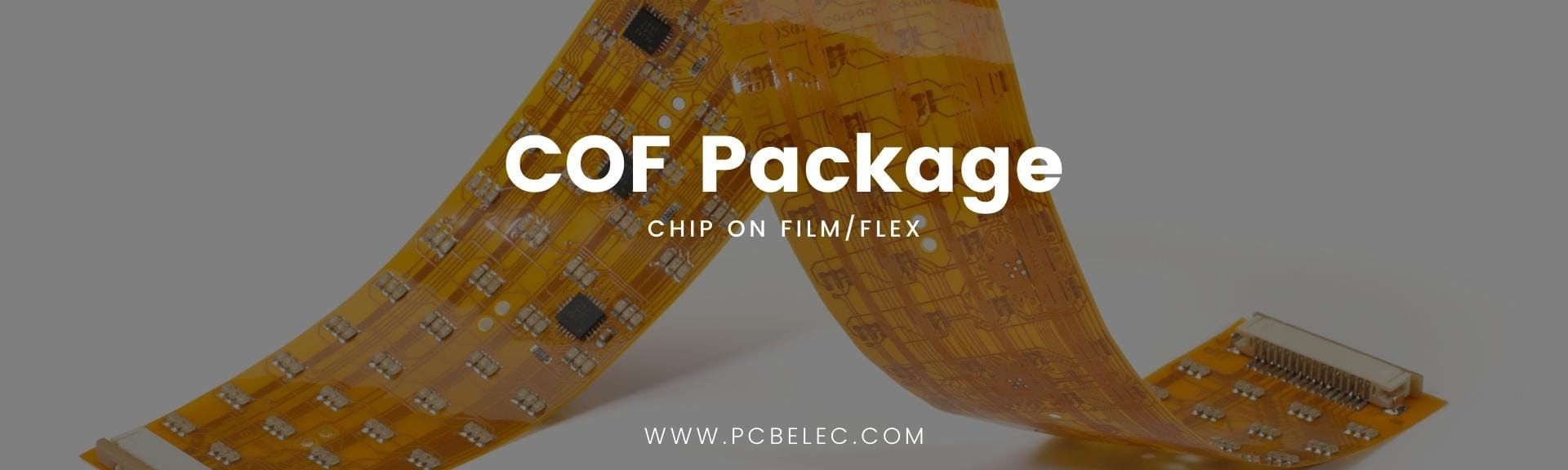
COF (Chip On Film/Flex), the chip is directly mounted on the flexible PCB. This connection method has a high degree of integration, and the peripheral components can be assembled on the flexible PCB together with the IC. This is an emerging technology.
The advantage of the COF package in some applications is to reduce package interconnection. Flexible circuits can be made with fine line width and line spacing, which can meet the requirements of wiring and connecting chips on one side and using another layer to meet the needs of grounding and shielding.
COF technology is mainly used in mobile phones or for PDP (plasma display) driver ICs, and other small LCD products. COF is the same as TAB and COG products. In addition to the Bonding IC on the COF Film, other parts such as resistors and capacitors can also be soldered on the circuit board, which can reduce the space occupied by the IC-related circuits; except for the components area that cannot be folded, the rest of the parts All are foldable.
COF has a simple structure, can be automatically produced, reduces labor costs, relatively reduces module costs, and has higher reliability than COG (such as thermal shock, constant temperature, and humidity, etc.). COF has a two-layer structure (Cu+PI), and there are no component holes on the product. Its overall thickness is thinner, its flexibility is better, and its peel strength is better. It is the future development trend of flexible packaging substrates.
The advantages of COF are:
- Smaller size, thinner and lighter;
- The chip is facing down, and the line spacing is fine, which increases the reliability;
- Regional reflow soldering can be done on the substrate;
- High bending strength;
- Passive components can be added;
- The number of pins can be reduced to half of TAB.
Optoelectronic Packaging

Optoelectronic circuit packaging poses a significant challenge to today’s packaging technology. Compared with other assembly technologies, it has stricter requirements on mechanical properties. Similarly, proper electrical performance requires impedance control of high-speed lines during circuit design. Flexible circuits are an ideal way to meet the needs of optoelectronic packaging. The potential disadvantages of FR-4 laminates for optoelectronic devices are the high dielectric constant of FR-4, high dielectric loss, and signal transmission delay in multi-high frequency systems.
Compared with FR-4, flexible circuits have improved material properties and have been used in current optoelectronic packages. PI insulating materials are commonly used in high-end applications of flexible circuits. The dielectric constant of this material is between 3.2 and 3.6, depending on different materials and test conditions, while the dielectric constant of FR-4 is 4.3 to 5.0.
The ability to make line widths and spacings less than 50um is improved, increasing the attractiveness of flexible circuits. The thin and flexible mechanical properties meet the needs of designers in package design. The thin cross-section (approximately 115um thick) allows the circuit to be easily connected to the heat sink or reinforcement material, providing good heat treatment capability and rigidity.
The mechanical and electrical properties of flexible circuits can meet the needs of optoelectronic packaging technology. They may also be one of the most significant growth points for high-density flexible circuits in the future.
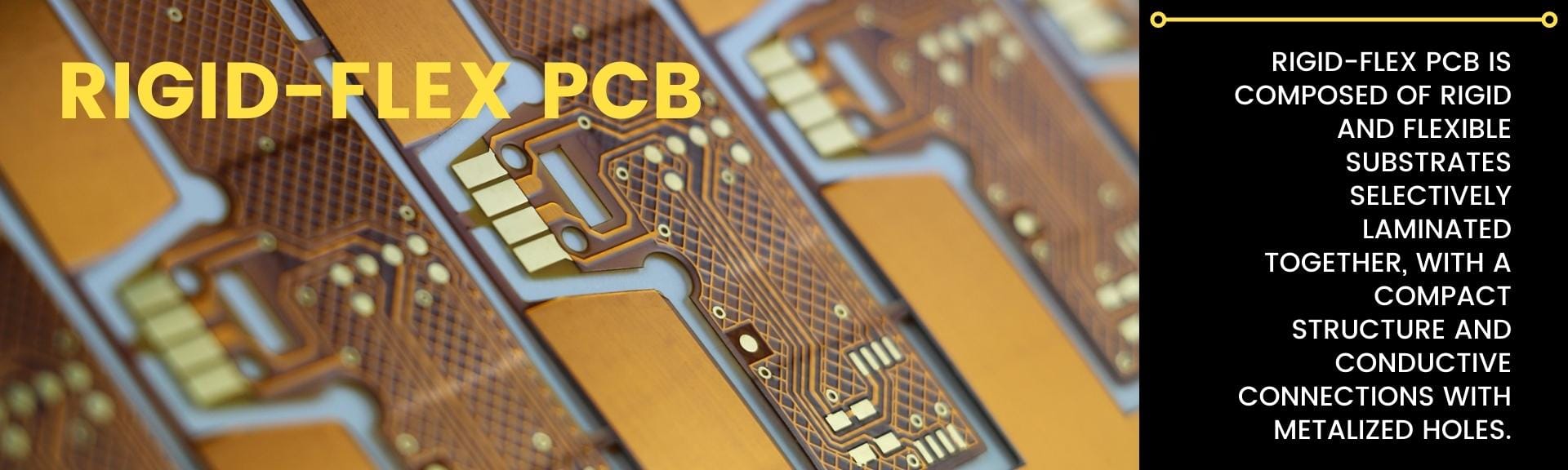
Rigid-flex PCB
As consumer electronics products, especially mobile phones and digital products, are lighter, thinner, and shorter, they continue to reduce the size of the finished product by reducing components or combining them into modules, resulting in the demand for rigid-flex PCBs. With rigid-flex PCB, connectors are unnecessary, and the product volume can be reduced. As far as the current digital image transmission is concerned, standard connectors will affect the transmission speed. Therefore, rigid-flex PCB must replace the connector to avoid transmission interruption.
Rigid-flex PCB is composed of rigid and flexible substrates selectively laminated together, with a compact structure and conductive connections with metalized holes. Each rigid-flex PCB has one or more rigid areas and one or more flexible areas. The rigid-flex PCB component manufactured by combining rigid materials and flexible materials takes advantage of the characteristics of flexible PCBs and solves the electrical connection problem with rigid PCBs.
Impedance Control
The resistance encountered in the transmission of the signal line is called the characteristic impedance. For high-speed signal lines, the characteristic impedance must be controlled within a specific value range so that high-frequency signals smoothly, which is commonly referred to as impedance control. For high-speed signal transmission, impedance control is often required. The optoelectronic devices and connectors of supercomputers require impedance control. There are several different structures for transmission lines (which are composed of signal lines, dielectric layers, and ground layers). Double-sided flexible circuits may be used less frequently. The two most commonly used structures in practical applications are surface microstrip and buried microstrip. ) Is related to the dielectric constant (DK). The surface microstrip line of one of such transmission lines is shown in the figure below.
The relationship between characteristic impedance and wire width () 1/2 oz, Cu, εr=3.4.
To improve packaging efficiency, the thickness of the designed dielectric layer needs to be reduced. However, to maintain the expected value of the characteristic impedance, the line width, thickness, and dielectric constant must be controlled.
Since flexible circuits can produce narrow and thin circuits, the characteristic impedance value can be adjusted to meet packaging requirements, which is more accessible than other packaging methods to a certain extent.
Summary
The characteristics of flexible circuits are very suitable for some applications that require high-density interconnection between components in the system. The forming ability for installation and connection, the precision ability of high-density circuits, the variety of heat treatment, circuit terminal selection, and the effective use of materials and space make flexible circuits extensive application prospects in current and future packaging applications.
Recommended Reading
- The terms you have to know related to the manufacture of Flexible PCB
- Complete Introduction To Flexible PCB Assembly Process
- What is Flexible PCB Prototype?
- 16 Factors Affecting The Cost And Price of Flexible PCB
- Knowledge of Plating on Flexible Circuit Board Surface
- Knowledge of Flexible Printed Circuit Board Processing Technology
- Key Process Flow of Rigid-Fled PCB Production


