
Complete Introduction to Flexible PCB Assembly Process
JHYPCB is a professional PCB manufacturer, providing prototype manufacturing and assembly services for single-sided, double-sided, and multilayer Flexible PCB.
Home » PCB Assembly » Complete Introduction to Flexible PCB Assembly Process
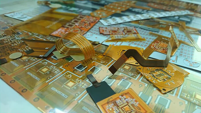
Flexible PCBs are a critical component used in a wide range of electronic devices, from smartphones and tablets to aerospace applications. With their compact size and lightweight design, flexible PCBs provide a reliable and efficient solution for connecting various components. However, with so many options available for their assembly, it can be challenging to choose the right method. This article will delve into the key steps involved in the flexible PCB assembly process, including substrate material selection, through-hole and surface mount technology placement, soldering, and testing and quality control. By following industry-standard best practices and utilizing advanced equipment and inspection techniques, we can ensure that the final product meets the expected performance standards.
What is Flexible PCB?
Flexible Printed Circuit Board is a type of circuit board that can be bent, folded, and rolled up. Compared with traditional rigid PCBs, they are thinner, lighter, and more flexible in shape. They are made up of flexible base materials and conductive circuits through special processing techniques and technologies to achieve flexibility.
Application Scope of Flexible PCB
Flexible PCB has become an indispensable part of many electronic device fields, such as mobile devices, consumer electronics products, medical equipment, etc. Because flexible PCBs have excellent adaptability and flexibility, they can be designed into various shapes and sizes to adapt to various space limitations and special requirements. For example, they can be integrated into compact electronic devices or used to connect various modules and components.
Advantages and Limitations of Flexible PCB
Compared with traditional rigid PCBs, Flexible PCBs have the following advantages:
- Lightweight and Thin: Flexible PCB is lighter and thinner than rigid PCB, making it suitable for use in devices with small space limitations.
- Flexibility: Flexible PCB can be bent, folded, and rolled up, adapting to various complex shape requirements.
- Diverse Wiring: Compared with rigid PCBs, Flexible PCB can be wired in any direction and angle according to needs.
- Excellent Electrical Performance: Flexible PCB has excellent electrical performance such as high-frequency transmission, impedance control, etc.
However, during the actual production process, Flexible PCBs also have some limitations:
- High Cost: Due to the high manufacturing cost, the unit price is relatively high, and the processing technology requires high demand.
- Difficult Design: Due to its flexibility and complexity, the design of flexible PCB is relatively more challenging, requiring experienced designers and technical personnel.
- Poor Durability: Compared with rigid PCBs, the durability of Flexible PCB is not as good as the latter. It’s also not suitable for high repetition bending scenarios.
Related Reading:
Introduction To Flexible PCB Assembly Process
I. Preparation Work Before Flexible PCB Assembly
- Selecting the Most Suitable Substrate Material
Flexible PCBs are made up of flexible base materials and conductive circuits. The choice of substrate material determines the overall flexibility and durability of the entire circuit board. Common substrate materials for flexible PCBs include polyimide (PI), polyester (PET), and polyethylene naphthalate (PEN). Each of these materials has different characteristics and is suitable for different applications. For example, PI material has a high-temperature resistance and excellent mechanical strength, making it ideal for use in harsh environments such as aerospace and military applications. PET material, on the other hand, is relatively inexpensive and widely used in consumer electronics products.
When selecting a substrate material, it’s essential to consider factors like temperature resistance, flexibility, and mechanical properties, as well as the application scenarios. Only by choosing the most suitable substrate material can we ensure the final product’s quality and performance.
- Checking If The Design Drawing Meets The Requirements
Before beginning the assembly process, it’s crucial to check whether the design drawing meets the requirements. Different types of PCB designs have different requirements, such as trace width, pad size, hole diameter, etc. Ensure that all design specifications meet the manufacturer’s requirements before production. It’s also essential to carefully review the design layout to avoid layout errors that may affect the functionality of the final product.
- SMT And THT Components
SMT and THT components are two types of organic electronic components that need to be prepared before assembly.
SMT components are placed directly on the surface of the PCB and soldered onto the conductive circuits using solder paste. They require less space than THT components and are suitable for small PCBs.
THT components have leads that pass through the holes on the PCB and then soldered to the conductive circuits. They require more space than SMT components and are commonly used in larger PCBs.
Before assembly, ensure that all SMT and THT components are properly prepared and meet the manufacturer’s specifications.
II. Flexible PCB Surface Mount Technology (SMT) Assembly Process
SMT assembly is the most common method used to assemble flexible PCBs. It involves placing surface mount components directly on the surface of the flexible PCB and then soldering them onto the conductive circuits using solder paste. The SMT assembly process can be broken down into three primary steps:
1. SMT Component Placement
The first step in the SMT assembly process is to apply a layer of solder paste to the conductive pads on the flexible PCB. Solder paste is a mixture of tiny solder balls suspended in a flux medium. The flux helps to clean the surface of the conductive pads and prevents oxidation during the soldering process.
After applying the solder paste, the SMT components are placed on the paste at their designated locations. High-speed pick-and-place machines can place SMT components quickly and accurately. Before placement, it’s essential to verify that all components are free from damage and contaminants that could affect the final product’s quality.
2. Soldering
Once all SMT components have been placed on the solder paste, the next step is to solder them onto the conductive circuits. There are several types of soldering methods available, such as reflow soldering, wave soldering, and selective soldering.
Reflow soldering is the most commonly used method for SMT assembly. It involves heating the entire assembly using a conveyor oven or a reflow oven until the solder paste melts and forms a bond between the component and the pad. The temperature profile must be carefully controlled to avoid overheating or underheating, which could cause defects like tombstoning, voids, or cold joints.
Wave soldering is an alternative method that uses a wave of molten solder to attach the components to the PCB. This method is not ideal for SMT components but can still be used with some through-hole components.
Selective soldering is a newer method that uses a robot-controlled nozzle to apply solder only to specific areas of the assembly. This method is useful for assemblies with complex shapes and reduces the risk of overheating or underheating.
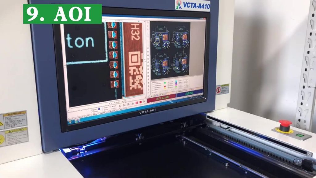
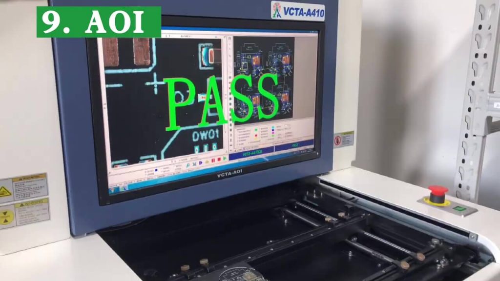
3. Inspection
After SMT placement and soldering, the final step is inspection. AOI (Automated Optical Inspection) and X-ray inspection are two popular methods for inspecting SMT components.
AOI uses optical cameras and advanced software algorithms to detect any defects or faults in the placement or soldering of SMT components. It provides a fast and accurate inspection that can identify problems like missing components, wrong polarity, skewed placement, or insufficient solder.
X-ray inspection, on the other hand, uses X-rays to view the internal structure of the assembly and identify any hidden defects. This method is especially helpful for detecting issues with ball grid array (BGA) components.
In summary, the SMT assembly process requires careful attention to detail at every step to ensure a high-quality final product. By following industry-standard best practices and using advanced equipment and inspection techniques, we can achieve reliable and consistent results.
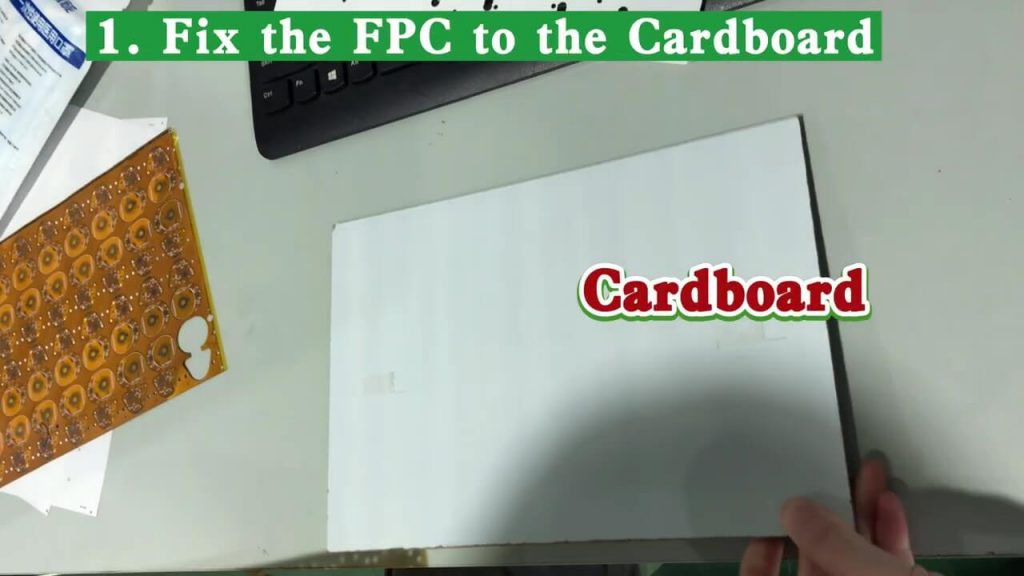
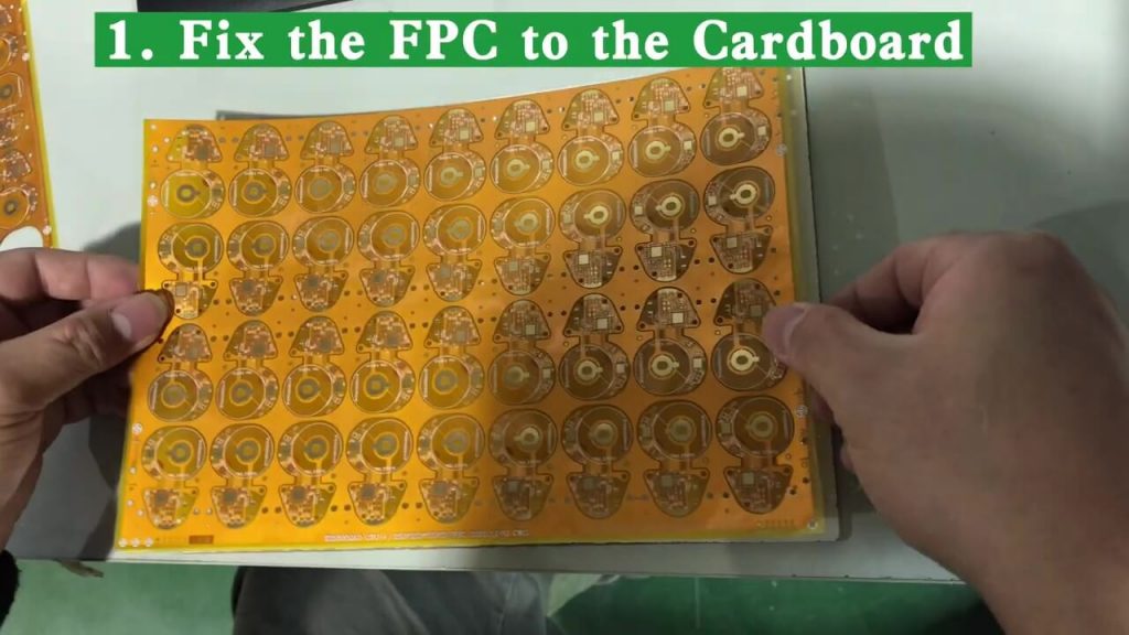
There are two ways to fix the Flexible PCB on the carrier board:
a. Single-sided tape fixation: Fix the four corners of the flexible PCB on the carrier board with high-temperature single-sided tape, and no FPC offset, or warping is allowed. The viscosity of the tape must be moderate, it must be easily peeled off in the subsequent process, and there must be no residual glue left on the FPC.
b. Fixing with double-sided tape: first, stick the high-temperature resistant double-sided tape on the carrier board, and then paste the FPC on the carrier board. In particular, it should be noted that the viscosity of the tape also needs to be moderate; otherwise, it will easily cause the FPC to tear when it is peeled off later.
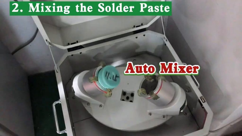
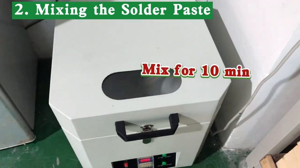
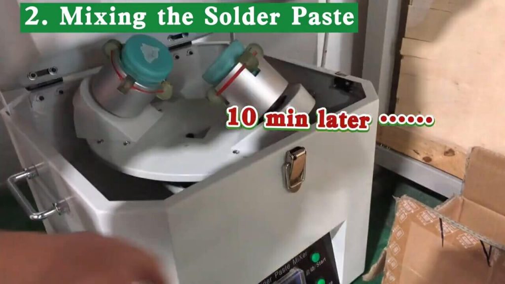
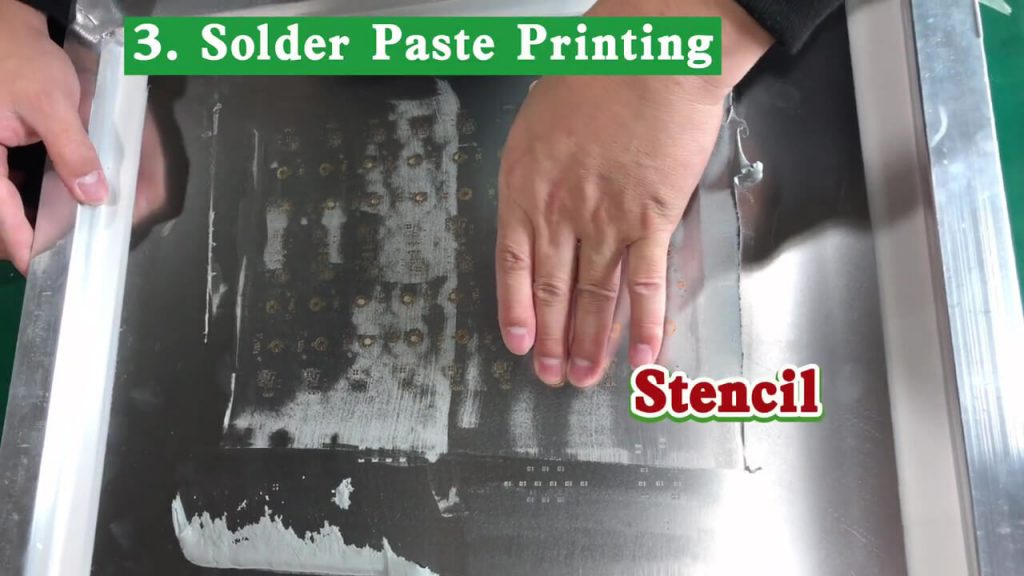
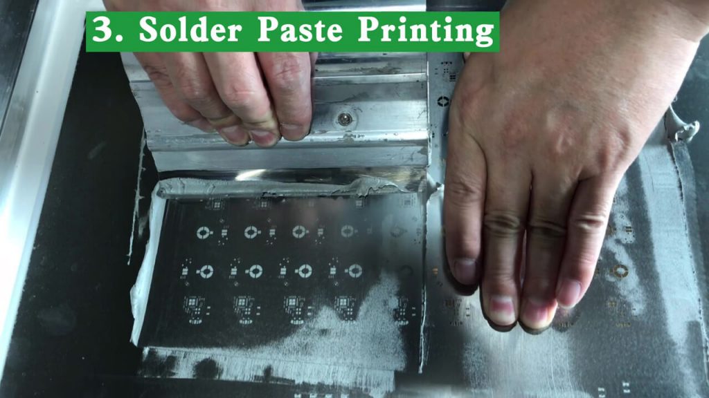
FPC has no special requirements for the solder paste composition, but it has higher requirements for the printing performance of the solder paste. The solder paste should have good thixotropy, can be easily demolded, and can be firmly attached to the surface of the FPC pad. There should be no problems such as poor demolding, blockage of the stencil opening, and collapse after printing.
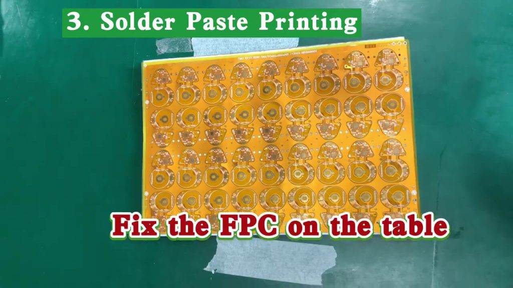
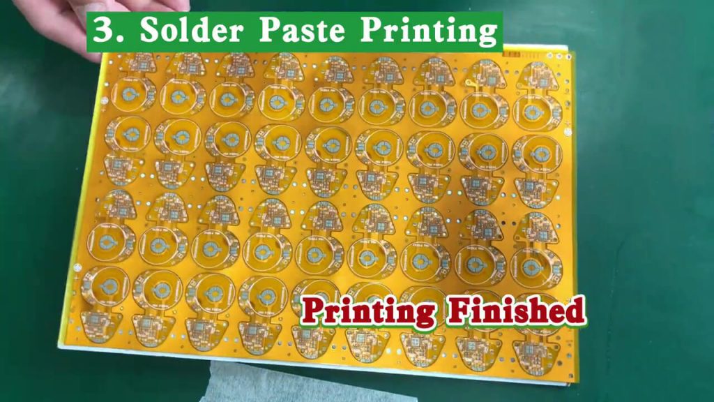
Solder Paste Printing
First, fix the FPC on the table.
Secondly, with the help of the SMT stencil, the solder paste is transferred to the pads of the flexible circuit board.
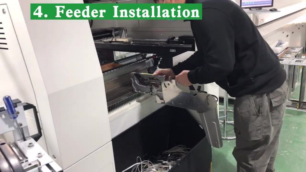
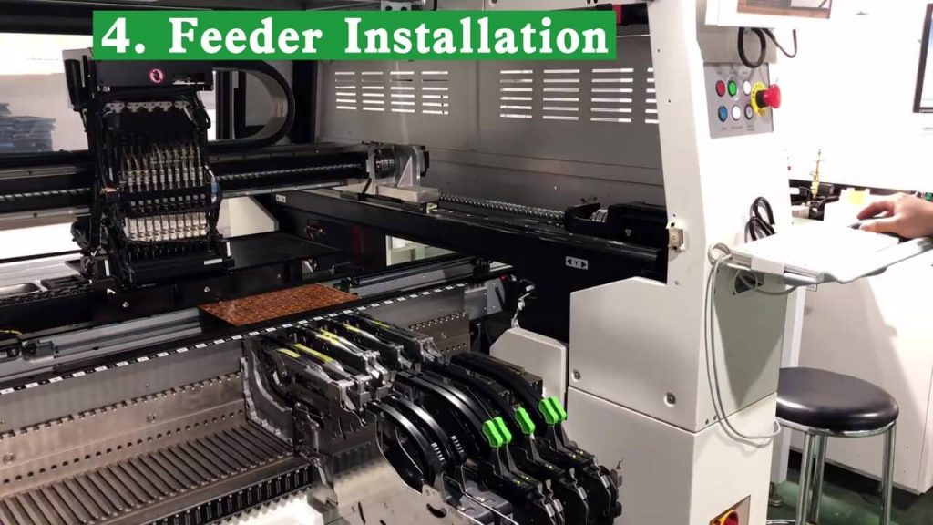
Feeder Installation
Feeder facilitates the surface mount components pick and place.
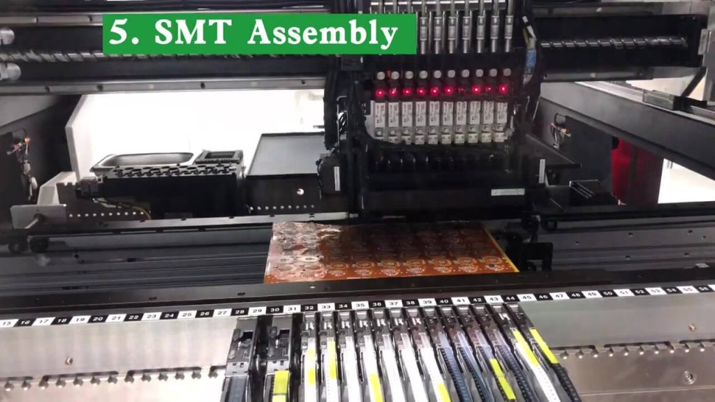
SMT Assembly
We use medium and high-speed placement machines for placement according to the product’s characteristics, the number of components, and the improvement of placement efficiency. Since there is an optical MARK positioning mark on each flexible PCB, there is almost no difference between SMD mounting on FPC and mounting on Rigid PCB.
It should be noted that although the flexible PCB is fixed on the carrier board, the surface of the flexible PCB is still not as flat as the rigid PCB. Therefore, the nozzle drop height and blowing pressure of the placement machine need to be accurately set, and the nozzle movement speed also needs to be reduced. This requires the placement machine to have the BAD MARK recognition function.
III. Flexible PCB Through-Hole Technology (THT) Assembly Process
THT assembly is another common method used to assemble flexible PCBs. This method involves placing through-hole components with leads that pass through the holes on the PCB and then soldering them onto the conductive circuits. The THT assembly process can be broken down into several primary steps:
- THT Component Placement
The first step in THT assembly is to place the through-hole components at their designated locations on the flexible PCB. Double-check that all components are free from damage and contaminants that could affect the final product’s quality.
- Component Lead Trimming
After placing the components, the excess component leads protruding from the bottom of the PCB must be trimmed to prevent short-circuits during soldering. Use a pair of diagonal cutters or an automated trimming machine to cut the leads as close to the solder joints as possible.
- Wave Soldering
Once the component leads have been trimmed, the next step is wave soldering. In this process, the PCB is passed over a wave of molten solder that flows through the holes on the PCB and forms a bond between the component leads and the conductive circuits. The temperature and speed of the wave must be carefully controlled to ensure complete coverage of the solder pads without overheating or underheating the assembly.
- Inspection
After wave soldering, the final step is inspection. Visual inspection, AOI, and X-ray inspection are three popular methods for inspecting through-hole components.
Visual inspection involves visually inspecting the assembly for defects like incomplete solder joints, solder bridges, or misaligned components.
AOI uses optical cameras and advanced software algorithms to detect any defects or faults in the placement or soldering of through-hole components. It provides fast and accurate inspection and can detect problems like missing components, wrong polarity, or skewed placement.
X-ray inspection uses X-rays to view the internal structure of the assembly and identify any hidden defects. This method is especially helpful for detecting issues with complex BGA components.
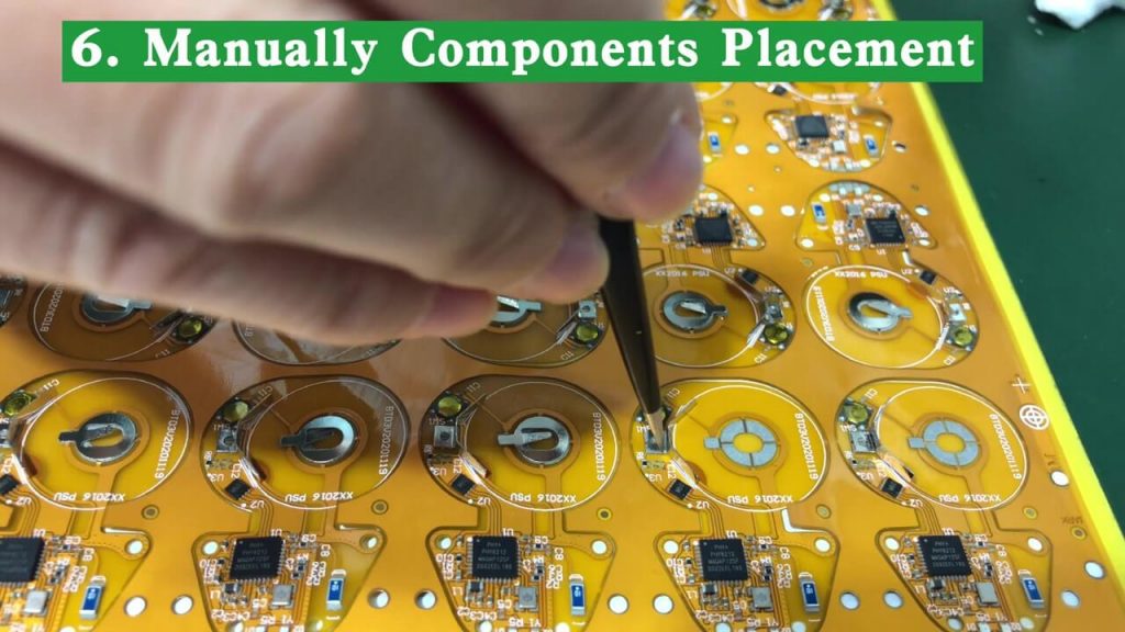
Manually Components Placement
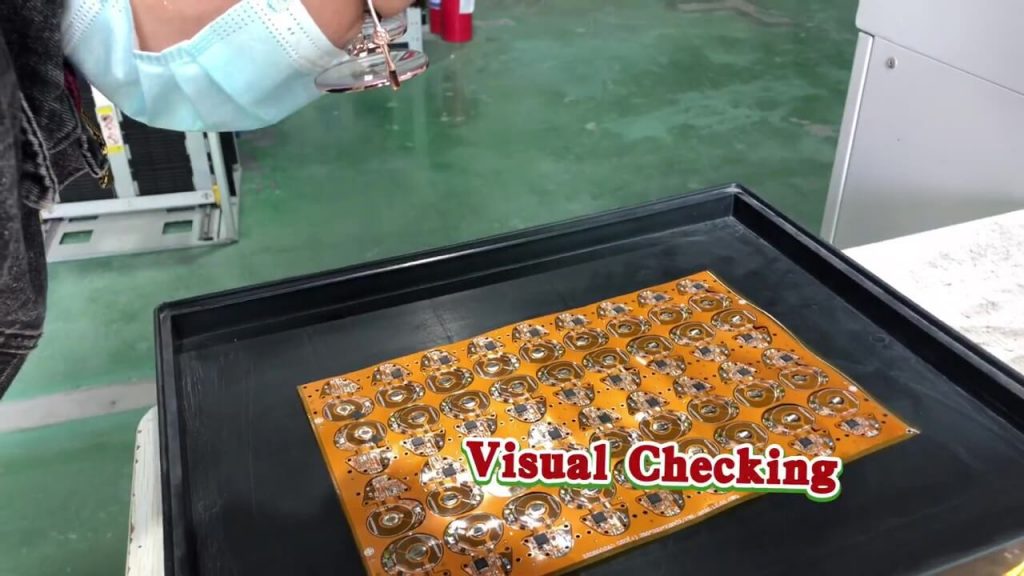
After the SMT assembly is completed, the placement of the manual components starts. Visual checking is required before the start of manual components placement. After the Visual checking is confirmed to be correct, the electronic components that cannot be completed by the automatic placement machine can be manually placed on the pads.
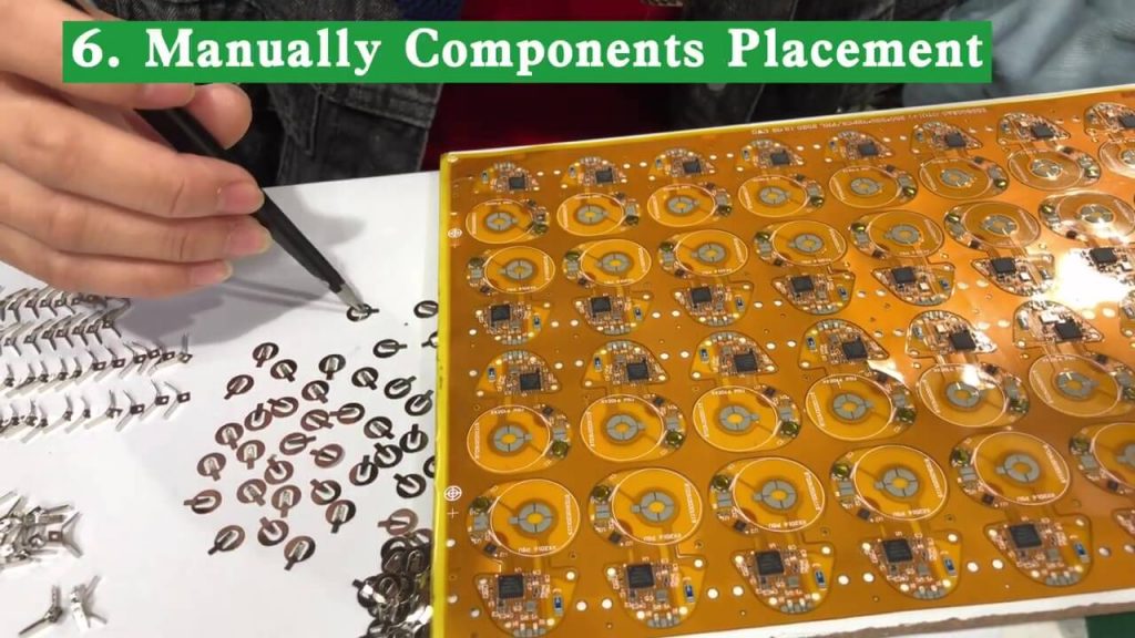
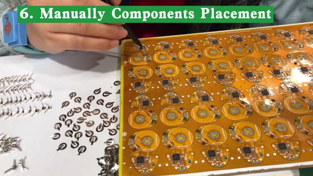
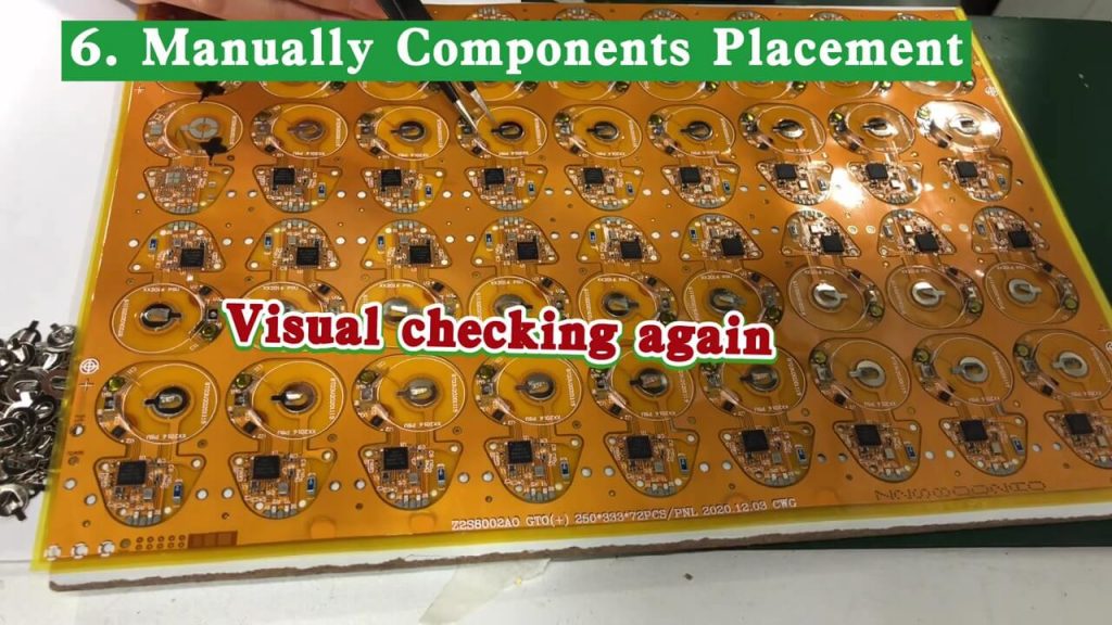
After the Manually components placement is completed, visual checking is required again.
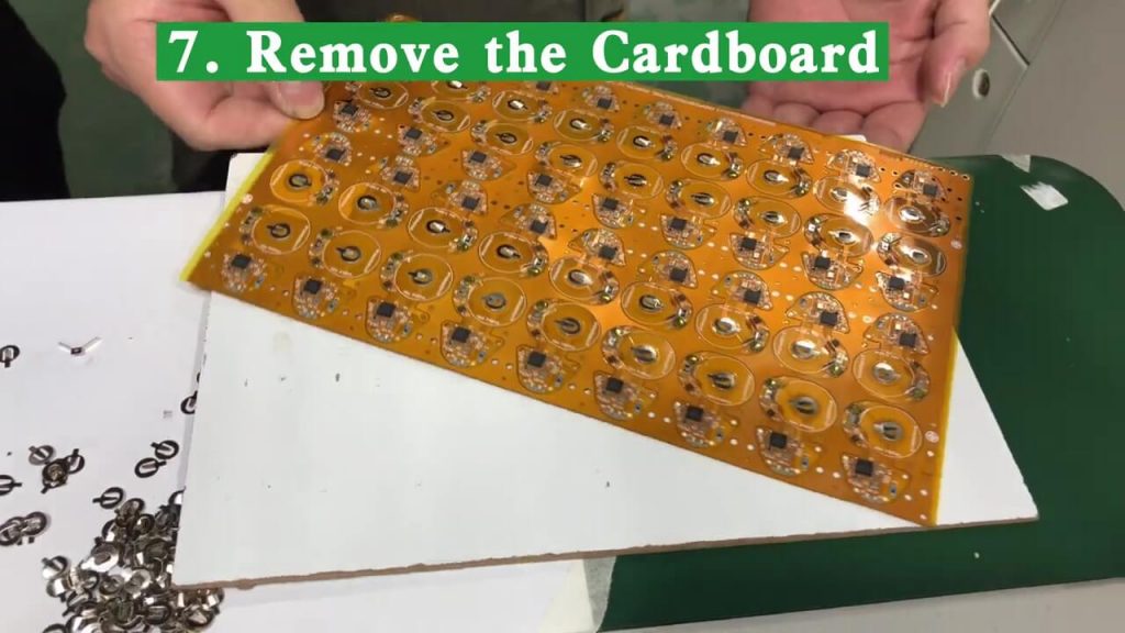
Remove the cardboard
Be careful when removing the FPC from the carrier board to prevent tearing.
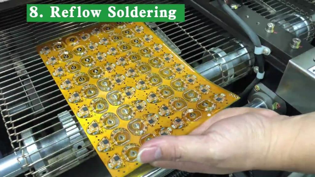
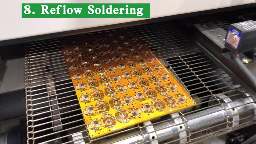
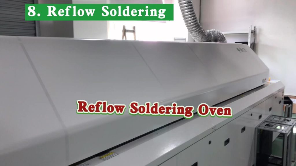
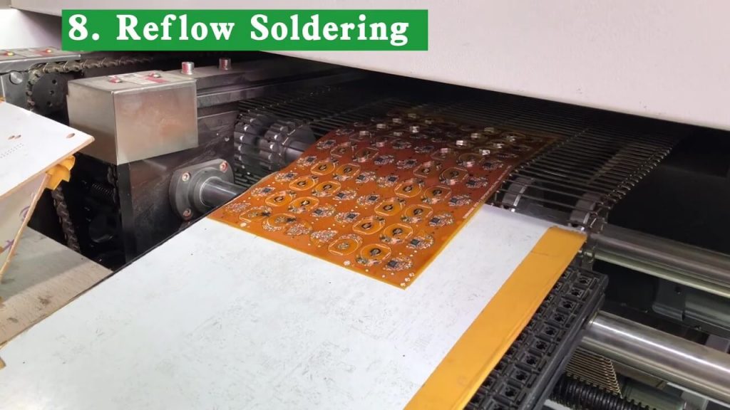
Reflow Soldering
For flexible PCB assembly, the use of a forced thermal convection infrared reflow oven can make the temperature change on the FPC more uniform. It can also effectively reduce the occurrence of poor soldering.
Related Reading: What is the difference between wave soldering and reflow soldering?
IV. Testing and Quality Control for Flexible PCB
Testing and quality control are crucial steps in the assembly process to ensure that the final product meets the required specifications and performance standards. The testing and quality control process for flexible PCBs can be broken down into several primary steps:
- Visual Inspection
The first step in testing and quality control is visual inspection. Highly experienced technicians inspect the assembled PCBs visually to identify any major defects or issues like visible damage, misplaced components, or soldering defects. This inspection is critical and ensures that any issues are detected early on.
- Electrical Testing
After visual inspection, the next step is electrical testing. Several testing methods are available, including continuity testing, functional testing, and flying probe testing.
Continuity testing verifies that all conductive circuits on the PCB are connected as intended and no short circuits occur between them. Functional testing is done to check if the functionality of the circuit board performs as per the desired output. Flying probe testing is an automated test that uses a robotic arm with probes to check continuity between specific points on the PCB.
- Environmental Testing
After electrical testing, the next step is environmental testing. Environmental testing simulates the operating conditions of the final product and checks how the flexible PCB performs under different environmental conditions like humidity, temperature, and vibration. These tests help to detect any potential failure modes that could occur during actual use of the product.
- X-ray Inspection
X-ray inspection is another method used to inspect flexible PCBs. This inspection technique can be used to view the internal structure of the assembly and identify any hidden defects or issues like misplaced components, insufficient solder, or cold solder joints.
- Quality Control Process
In addition to testing, a robust quality control process is necessary to ensure that the final products meet or exceed the expected quality standards. A comprehensive quality control process should include a series of checks, including supplier quality control, incoming material inspection, in-process inspection, final product testing, and post-delivery support.
Supplier quality control involves evaluating the quality of materials and parts supplied by third-party vendors, while incoming material inspection involves checking all the components and materials used in the assembly process.
In-process inspection involves monitoring the assembly process at each stage to ensure that it meets the required specifications. This inspection helps detect any issues early on to prevent them from propagating further through the manufacturing process.
Final product testing is done after assembly to ensure that the assembled PCBs meet or exceed the expected performance standards. Post-delivery support includes providing assistance and support to customers in case of any issues with the final product.
Related Reading:
Punching
After the flexible PCB is produced, most of each piece is connected. After the assembly is completed, we need to cut it into single pieces. We recommend making a special FPC punching abrasive tool for punching and dividing the board. This can significantly improve work efficiency. At the same time, the edges of the punched flexible circuit boards are also neat and beautiful. The internal stress generated during punching is very low, effectively avoiding solder joint cracking.
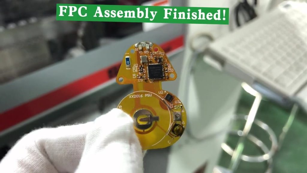
At this point, the flexible PCB assembly has been completed. In the process of flexible electronic assembly, accurate positioning of FPC and reasonable fixed quality assurance are the keys. The flexible PCB assembly process, the pre-baking, solder paste printing, patching, reflow soldering, etc., of the flexible PCB, are pretty different from the rigid PCB assembly process. The difficulty is also more incredible. To ensure the final quality of flexible PCB assembly, each process must be strictly implemented following various regulations and the best quality control work.
The essential equipment and materials required for flexible PCB assembly include solder paste, SMT stencil, carrier board, dust-free cloth, gloves, solder paste mixer, solder paste printer, placement machine, reflow oven, cleaning machine, magnifying glass, AOI tester, ICT and FCT test fixture, etc. Different PCB assembly plants have different equipment and quantities.
V. Summary
Flexible PCBs are an essential component in a wide range of electronic devices. They offer a compact and lightweight solution to connect and integrate various components, making them ideal for use in wearable devices, medical devices, and aerospace applications. The assembly process for flexible PCBs involves several critical steps, including selecting the right substrate material, through-hole and surface mount technology placement, soldering, and testing and quality control.
A successful flexible PCB assembly process requires careful attention to detail at every stage, from initial design to final inspection. By following industry-standard best practices and using advanced equipment and inspection techniques, we can achieve reliable and consistent results that meet or exceed the expected performance standards.
Recommended Reading
- Full Turnkey LED PCB Board Manufacturing and Assembly Services in China
- Through Hole PCB Assembly
- Fast Prototype PCB Assembly Service
- Low Volume And Quick Turn PCB PCB Prototype Assembly Services
- How to Use PCB Stencil-Step by Step Guideline
- How To Clean The Solder Paste On SMT Stencil
- What is the Bill of Materials(BOM), and how to create one?
- The Production Process and Specifications of PCB SMT stencil
- Knowledge of Flexible Printed Circuit Board Processing Technology
- The terms you have to know related to the manufacture of Flexible PCB
- How to Solder On Flex PCB?
- Choosing the Right PCB Assembly Manufacturer for Your Needs
- Leveraging Turnkey PCB Assembly Manufacturing Services
- Evaluating and Selecting Quick-Turn PCB Assembly Manufacturers in China
- Shenzhen – The Global Hub for High-Quality PCB Assembly Manufacturing