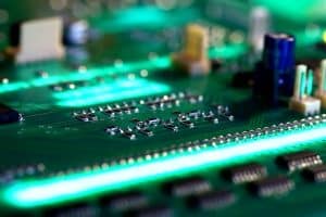
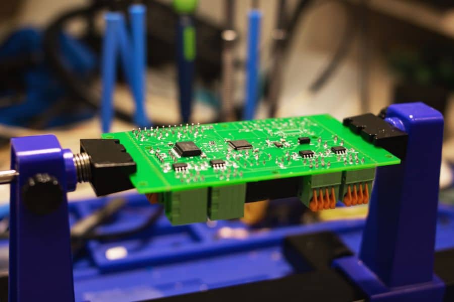
Developing new electronics products requires iteratively building and testing PCB prototypes. However, PCB prototyping can be expensive, with professional fabrication quickly running up large bills. When you’re making frequent iterations during the design process, these costs add up rapidly. This deters makers and startups who need to prototype on a budget.
Fortunately, by carefully optimizing your PCB design and fabrication approach, it’s possible to build functional PCB prototypes at very low cost. Basic prototypes for simple boards can even be self-made at home using DIY techniques for under $50. Achieving these low-cost PCB prototypes requires understanding what capabilities you actually need for prototyping vs final fabrication.
In this blog post, we’ll explore various techniques for dramatic cost reduction when making PCB prototypes. We’ll compare options like budget manufacturing vs DIY home fabrication. You’ll also learn PCB design guidelines tailored for low-cost rapid PCB prototyping. Following these principles allows optimizing designs early for fast fabrication and iteration at minimal expense. By utilizing these strategies, makers and entrepreneurs can enable more rapid testing of more design concepts without breaking the bank.
Table of Contents
Setting a Realistic Budget for Your PCB Prototype
When embarking on creating a new hardware product, many inventors fail to properly budget for designing, prototyping and iterating their PCB Concepts. However, setting clear cost expectations early is crucial for managing product development costs. Rushing through the design process without budget awareness often results in unnecessary expenditures from excessive changes late in development.
For simple, two-layer PCB boards under 50 square cm, basic functional prototypes can realistically be obtained for under $50 per board if optimized correctly. As board complexity and size increases into 4-6 layers spanning larger form factors, realistic budgets would be around $200-300 per prototype iteration. High-complexity boards with dense BGAs and HDI technology can quickly require $2,000-5,000 or more per prototype. However, the majority of early-stage consumer devices likely do not demand this level of sophistication.
One technique for maximizing the prototyping budget is to evaluate each PCB characteristic to understand cost impacts. Size is one of the foremost drivers – minimizing form factor reduces both material and fabrication costs substantially. The substrate itself also majorly affects budgets, with exotic materials like Rogers increasing costs exponentially over standard FR-4 designs. Minimizing layers is another critical guideline, as each additional metal layer adds significant expense in both board fabrication and the complexity of electrical testing. Finally, avoiding dense component areas through wider trace/space rules and larger package sizes also saves considerably.
By realistically scoping budget at the onset around key parameters like size, material, layer count and component complexity, inventors can allocate adequate prototyping runways. Carefully tailoring designs to essential functionality prevents “gold-plating” boards early, while still enabling sufficient testing to progress the product concept. Building even basic prototypes truly on a shoestring presents other challenges though – understanding tradeoffs between budget professional services vs DIY home fabrication enables finding the optimal approach tailored to your specific product’s needs.
Options for Low-Cost PCB Prototyping
When optimizing for low cost PCB prototyping, you have two fundamental options: budget professional circuit board manufacturing or do-it-yourself fabrication. Each method has key tradeoffs to consider regarding capabilities, costs, and ease of use. Budget professional companies in China have introduced disruptively inexpensive production to the electronics space, while the emergence of makerspace communities have democratized self-built designs, albeit with capabilities limits. Carefully evaluating each method is critical to finding the optimal path to fast affordable PCB iterations.
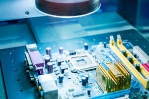
Budget Fab Houses in China
Chinese PCB manufacturers now offer impressive capabilities at unbeatable prices. Using these established fabrication houses is a proven path to low cost PCB board multiplication once your design is finalized. However, not all board houses in China are created equal. You must carefully investigate process capabilities, cost structures, quality programs, and engineering support. Dialectic impediments can also complicate file transfers and technical discussions. Choosing the right partners with extensive experience supporting foreign startups is key.
Recommended China Prototype Partners:
- JHYPCB
- PCBWay
- JLCPCB
- EASYEDA
- MyroPCB
Consolidated Freight Forwarding Services
For very small quantities under 5 boards, consolidated cross-border forwarding services can also significantly reduce costs. These middlemen pool small packages across customers for economics of scale in international shipping from China manufacturers. example is PCB Pool for aggregating prototypes and small series from low-cost Asian board houses. With clever consolidation, average costs can be as little as $30 per board shipped.
Self-Manufacturing Options
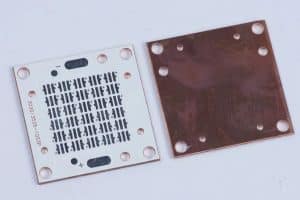
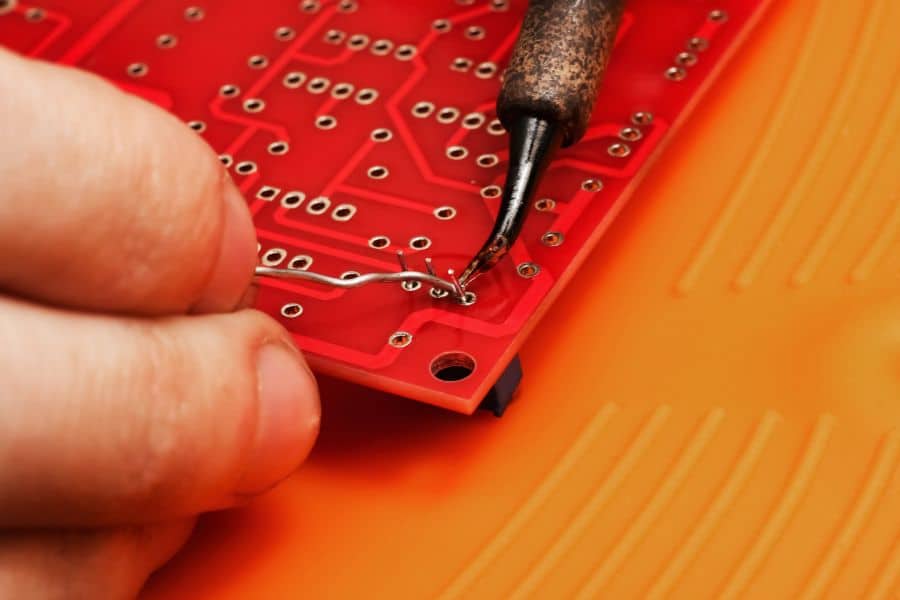
For the ultimate in cost savings, home-based manufacturing is an intriguing DIY option. While unable to match capabilities of industrial equipment, home etching and milling can enable surprisingly sophisticated results. Most methods use toner transfer for masking pattern designs burnt directly onto bare copper clad substrate, followed by chemical etching to shape conductors. Others directly mill traces mechanically. We’ll cover popular self-build options in the next section…
Self-Manufacturing Low Cost PCB Prototypes
For makers and inventors focused purely on minimizing expenditures, home-based PCB fabrication allows radical cost reduction in exchange for tolerating lower reliability and professional fit/finish. DIY manufacturing leverages manual masking and etching or mechanical milling for custom boards originating from your own workshop, not an industrial facility. While possessing numerous limitations, these techniques enable building working PCBs for under $50. We’ll survey popular self-build options.
Toner Transfer The most accessible DIY PCB process uses laser printer toner to transfer an etched resist mask onto blank copper clad substrate that is subsequently chemically milled. After printing the mask onto glossy paper, an iron transfers the toner onto the copper while heat fuses it. Areas protected by toner resist etching by ferric chloride or similar solutions. acetone removes toner after etching, leaving behind copper traces in the mask pattern.
Advantages:
- Extremely low materials cost
- Allows rapid design iteration
Limitations:
- Unable to achieve fine trace sizes below ~0.5mm
- Higher defect rates impacting reliability
Milling PCBs More ambitious makers directly mill traces instead of chemical etching using adapted CNC routers. Mechanical milling removes copper to isolate custom conductor patterns carved based on CAD toolpaths. Milling eliminates issues of toner transfer consistency, supports smaller geometries nearing 0.1mm, and avoids etching chemicals. However, the required CNC equipment has a steep cost and learning curve.
Advantages:
- No harsh chemicals
- Finer details than toner transfer
Limitations:
- High equipment cost
- Still unable to match pro grade tolerances
While home fabrication sounds appealing for radical cost cutting, consistency, and quality issues prevent an application for mass distribution. However, exploring DIY techniques allows education for designers on real world manufacturing processes when used judiciously.
Optimizing PCB Prototype Design for Low Cost Fabrication
When targeting extremely low cost PCB prototyping, particularly with home fabrication methods, optimizing the board layout and component selection requires additional considerations beyond typical design guidelines. Inventors can minimize unnecessary design iterations by accounting for inherent process limitations early when drafting prototypes aimed at budget production.
We’ll overview core principles that enable economical board designs:
Simplicity Foremost, remove any functionality not utterly essential for validating your core product concept to enable simpler board topologies. Minimize component counts, layer numbers, and form factors as much as possible.
Loose Tolerances
Avoid holding overly tight tolerances unnecessarily early in prototyping that would require expensive test & measurement equipment to validate. Allow for greater variances in parameters like impedances, dimensions etcetera.
Design Headroom
Additionally, provides ample spacing in trace width/separation rules, annular rings, solder mask expansion, and other critical dimensions. This ensures sufficient margin to account for reduced precision in home etched or milled PCBs that may suffer registration errors or undercut traces.
Standard Materials
When possible, design to industry standard thicknesses and materials like 1.6 mm FR-4 instead of more exotic substrates. Similarly, choose common copper weights (1 oz) unless higher current capacity unavoidable.
Easy Assembly
Lastly, design components to be easily hand soldered during assembly without expensive tools. Prioritize through-hole parts instead of challenging fine-pitch surface mount to allow generous keepout zones. Avoid BGAs or other high pincount packages.
While such guidelines constrain the design process, they enable cost efficient building of working prototypes for concept verification built either in small volumes from professional board houses or DIY fabrication. This facilitates developing products based on actual hands-on testing data rather than pure simulation or guesswork. Review any available design rule checks from your chosen PCB manufacturer to catch errors early also.
Working With PCB Prototype Manufacturers
To smoothly procure low cost printed circuit board prototypes, effectively partnering with your chosen board fabrication house, whether a budget Chinese vendor or local milling shop, accelerates progress. We’ll cover best practices in supplier communication, file exchanges, design reviews, and order management when externalizing PCB prototype manufacturing.
Communicating Requirements
Whether asking basic questions on capabilities or detailing complex board stackups, clearly conveying PCB prototyping needs is essential to avoid unnecessary delays or errors. Check provider datasheets and website FAQs first before inquiries. Use simple, direct language avoiding colloquialisms given potential language barriers. Have your Gerbers and drawings ready to illustrate needs visually.
Managing Gerber Data Exchanges
Supply all required Gerber and drill files per manufacturing guidelines to prevent problems. Confirm layer naming conventions match expectations, include all mechanical layers like assembly drawings. Always audit visual previews in CAM viewers like Gerbv yourself for errors before submitting files. For DIY paths, generate toolpath files required for your milling machine if applicable.
Design Reviews
For advanced projects with tight tolerances or high frequencies, request design reviews by engineering teams before fabrication if available. While reviews incur charges, getting guidance to tweak stackups, trace widths, and the like prevents costly re-spins. Be open minded to suggestions based on accumulated manufacturing expertise.
Ordering and Logistics
Carefully enter required order quantities, materials, thickness, finishes, lead times, and other parameters into order forms to prevent back/forth clarification emails. Maintain clear lines of communication as build processes commence, tracking order status milestones. Once boards ship, confirm transit & customs tracking info to estimate delivery, arrange handoff.
By upholding disciplined product data processes when engaging board partners for prototyping services, product makers save immense time and frustration. Solicit manufacturing input often as you navigate from prototypes towards eventual mass production as well.
Achieving Low Cost PCB Prototypes - Conclusion
In summary, inventors and startups can drastically reduce printed circuit board prototyping costs by:
- Realistically budgeting early for essential functionality vs unnecessary “gold-plating.”
- Weighing tradeoffs of budget factories vs DIY home fabrication
- Optimizing board layouts for simplicity, loose tolerances, and easy assembly
- Closely partnering with chosen manufacturers for smoothly procuring quality boards
Following these guidelines enable building working prototypes for under $50 in many cases – either through smart DIY techniques or utilizing new economy Chinese board houses. While no substitute for eventual higher-grade production, low cost prototypes empower small teams to pursue daring ideas despite limited funding.
Next Steps with JHYPCB
Here at JHYPCB, we specialize in providing radically affordable PCB prototype and small-batch manufacturing services to hardware entrepreneurs worldwide. With rigorous quality control and engineering-first focus, JHYPCB delivers reliable boards with leading-edge capabilities at up to 70% savings versus traditional vendors.
To learn more about actualizing your product ideas with low cost functional prototypes from JHYPCB, contact our engineering team today at sales@pcbjhy.com!
Related Reading