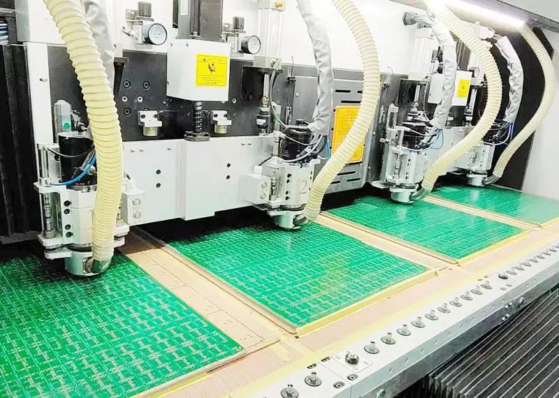
PCB prototyping is a critical step in the electronics design process. Quickly and affordably obtaining prototype PCBs enables designers to verify their circuits and product concepts early. However, to receive high-quality prototype boards in a timely manner, it’s important to understand the requirements and provide the necessary information to your PCB manufacturing partner.
When working with a PCB prototyping company, what are the key requirements designers need to fulfill to ensure a smooth prototyping process? Several important considerations around file formats, board layout, documentation, and more must be considered. Providing the fabrication shop with exactly what they need to manufacture quality PCB prototypes rapidly helps prevent delays and errors.
In this post, we’ll outline the essential requirements for PCB prototype manufacturing that designers should understand when planning their next project. Whether you’re looking for standard or quick-turn fabrication, being aware of the necessary files, design rules, specifications, and documentation will enable you to receive your prototype boards as efficiently as possible. Read on to learn how to set your next PCB prototyping project up for success.
Table of Contents
Type of PCB Board
The first thing that you need to decide is the type of PCB prototype. There are various types of PCBs available in the market. You can choose any of the PCB types according to your requirements. Let’s see some of the commonly used PCBs.
- Rigid PCB
The most common and oldest type of PCB is a rigid PCB. It is made from a hard substrate. These PCBs remain in their shape because of their hard material, and they cannot be bent. Bending these PCBs will break the board. So, they are used where bending is not required.
- Flexible PCB
Flexible PCBs, as the name suggests, are flexible. They can be bent easily. Due to their bending ability, they are widely used. You can use these PCBs in compact and unusual spaces. These are mostly used in UAV, LCD, projectors, cameras, wearable devices, printers, aviation instruments, etc. They are made from flexible materials such as polyester film, polyimide film, and fluorinated ethylene propylene film.
Advanced Learning:
- Rigid-Flex PCB
Rigid-Flex PCB is the intermediate version of both flexible and rigid PCB. This PCB has flexible layers as well as rigid layers.
Advanced Learning:
These PCBs are widely used nowadays. HDI stands for High-Density Interconnect. Therefore, it has a higher density of circuitry or electrical connections per unit area. So, the size of this PCB is very compact, and it is very lightweight. They have blind and buried vias that are less in diameter. The components are closely placed, reducing the transmission loss and allowing the signals to transmit faster. It is widely used in mobile phones, laptops, cameras, etc.
More Adventures: HDI PCB Layout and Basic HDI Design Guidelines
- And so on
Besides, there are LED PCB, Aluminum PCB, High TG PCB, etc. Please click here to learn more about the PCB products we can produce.
What File Formats Do PCB Prototyping Companies Accept?
When creating fabrication and assembly files for your PCB prototype, it’s crucial to provide them in a format acceptable to your manufacturer. Some companies are quite rigid about requiring one specific file type, while others allow more flexibility. Here are the primary file format options for PCB prototyping:
Gerber Files
By far, the Gerber file is the most common format requested by prototype PCB manufacturers. Gerber is an open standard for PCB layout data used since the 1960s. It breaks the design into multiple files – copper layers, solder mask, silkscreen, drill data, etc. Most PCB design software can export Gerber files today. Due to its universality and completeness, sending Gerber files is the safest bet for ensuring your prototyping partner has what they need to fabricate your boards.
CAD Files
Some PCB prototyping companies allow submitting the original CAD files from your EDA software rather than requiring exported Gerber files. This can speed up the process by avoiding manual Gerber generation. However, not all CAD tools are supported, so check with your manufacturer first. Converting the native CAD database directly to manufacturing machine instructions also bypasses potential Gerber interpretation issues.
PDF Files
While PDFs are easy to generate and share, they do not contain the detailed manufacturing information provided in Gerber or CAD files. Some basic board houses may accept PDFs, but it is not recommended for complex or high-density designs. PDFs can suffice for very simple PCB prototypes, but the lack of precision often results in errors.
What Design Rules Must Be Followed?
To ensure your PCB prototypes function properly and can be manufactured without issues, following basic PCB design rules and your manufacturer’s guidelines is crucial. Here are some of the most important design rules to keep in mind:
Trace Width and Spacing
Having trace widths and spacings between traces (clearances) that are too small can lead to shorts or reliability problems due to overheating. Most manufacturers will require minimum trace width and clearance rules based on the board thickness and voltages involved. Be sure to design according to their guidelines.
Annular Rings
The annular ring refers to the area of bare board surrounding a plated through-hole. If the ring is too small, the pad may lift or peel away from the board during soldering. A minimum annular ring size of 0.004” (0.1mm) or more is a good guideline.
Via Sizes
Vias, like traces, must meet minimum size requirements to avoid issues with hole filling or plating quality during fabrication. Typical minimum finished via sizes ranges from 0.2mm to 0.3mm. Follow your manufacturer’s recommendations.
Silkscreen Margins
The silkscreen layer should have adequate margins from pads, vias, and other features to prevent ink from bleeding onto copper. A minimum 0.003” (0.076mm) clearance is a good target.
Following basic PCB design rules upfront prevents your prototype fabrication and assembly headaches. Check with your PCB manufacturer on their specific minimum requirements.
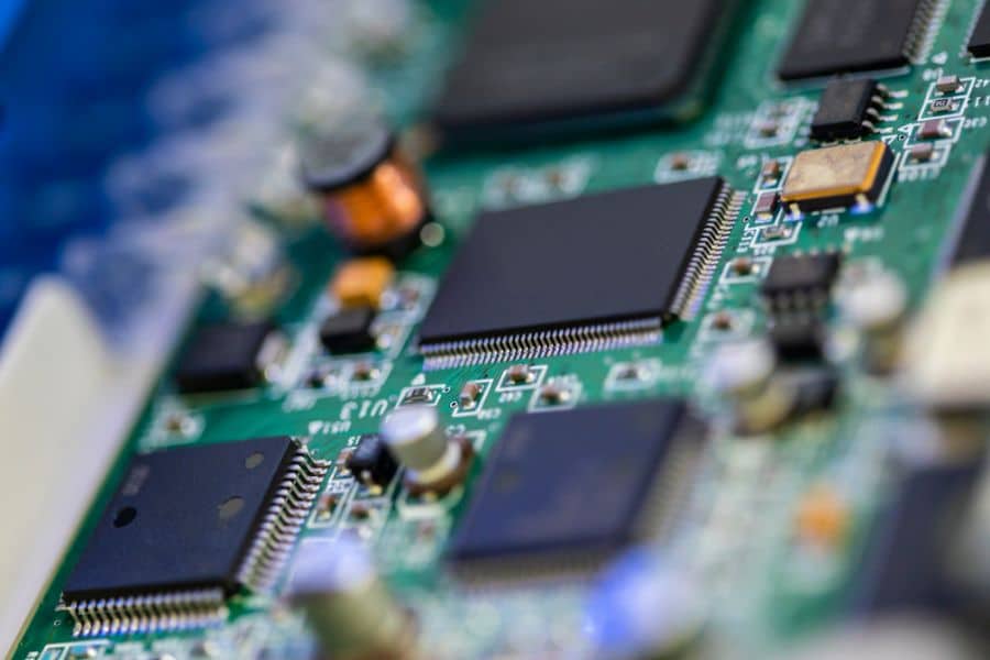
What Information Is Needed About Layer Stackup?
When ordering PCB prototypes, you’ll need to provide detailed information about the number of layers and materials used for your board’s layer stackup. This controls many characteristics of the finished boards. Details that must be defined include:
Layer Count
Simple boards may only require 2 layers, while complex designs may need 6 layers or more. The fabrication shop needs to know the total layer count. More layers allow greater routing flexibility but increase costs.
Materials
The substrate material for the PCB core and prepreg bonding layers needs to be specified. Common options are FR-4, Rogers, polyimide, etc. This impacts electrical performance and cost. Any special material requirements must be communicated.
Thickness
The thickness of the substrate core and copper layers must be defined. Thicker cores provide better heat dissipation and structural rigidity, while thinner cores save space and cost. Copper thickness affects current capacity and resistance.
Communicating details like the number of layers, stackup sequence, substrate materials, and layer thicknesses ensure your PCB prototyping partner can fabricate your design according to the right specifications. Leaving out this information can produce boards with incorrect layer configurations.
How Should Panelization Be Handled?
For PCB prototype orders, you’ll need to specify to your manufacturer whether you want individual boards or a panelized array of boards. Panelizing boards can significantly reduce prototyping costs but do require additional considerations.
Individual Boards vs. Panelized
If you just need a few PCB prototype boards, ordering them individually is simplest. But for higher quantities, getting boards panelized in an array and then broken apart after fabrication reduces cost. Be sure to specify your preference.
Tooling Holes
If requesting a panelized array, precision tooling holes must be designed in the panel for manufacturing purposes. Often, an array of 4+ holes is used. The holes allow for accurate localization of boards in the panel.
Mouse Bites
Small V-shaped etches called mouse bites are typically placed between boards to facilitate the break-apart process after panelization. Their dimensions and locations should be indicated in the layout.
Clearly specifying whether individual or panelized boards are required and providing panelization details upfront prevents errors and speeds up fabrication. Trying to panelize after prototype delivery increases time and cost. Discuss panelization requirements with your PCB manufacturer early in the prototyping process.
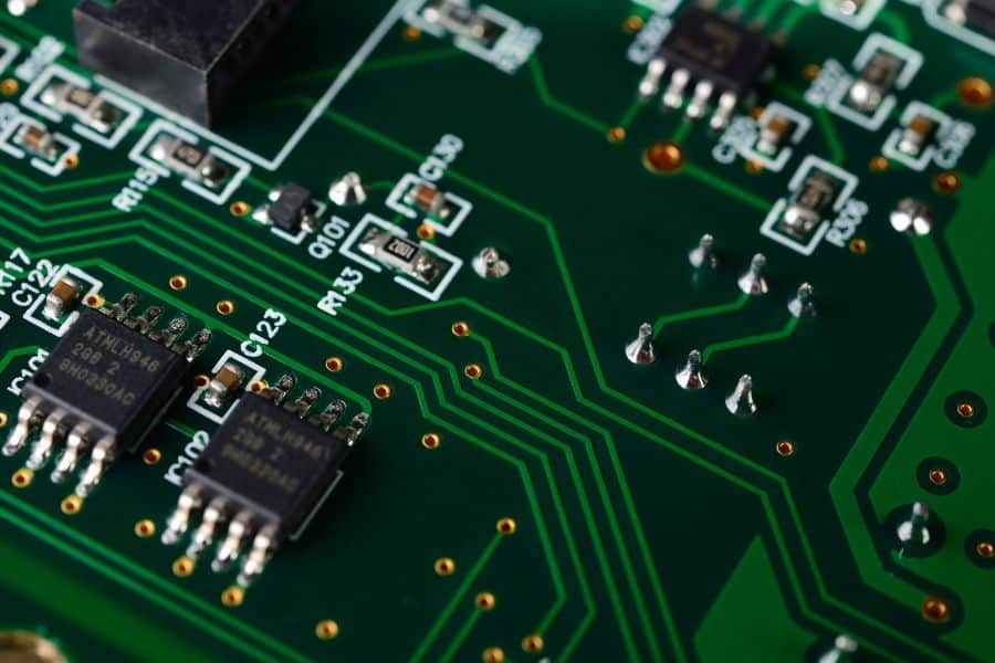
What Documentation Is Required?
In addition to the PCB layout and fabrication files, providing sufficient documentation helps ensure your prototype boards are manufactured and assembled properly. Key documentation to supply includes:
The BOM lists all components to be mounted on the assembled PCB. This allows the manufacturer to source the components and plan assembly steps. List part numbers, values, and quantities.
Assembly Drawings
Assembly drawings illustrate board layer stackup, component locations, board outline with tolerances, and any special assembly instructions. This provides clear visual information for manufacturing.
Test Procedures
If you require any testing of your prototypes, detailed test procedures will need to be provided. This includes parameters to be tested, test methods, required equipment, and pass/fail criteria.
Other Documentation
Any special requirements should also be communicated, such as requested lead times, solder masks, surface finishes, or packaging methods. Prototyping will go smoother with thorough documentation.
Supplying your PCB prototyping partner with complete documentation gives them all the information required to correctly meet your project’s fabrication, assembly, and testing needs. Missing documentation can easily result in mistakes or part-sourcing issues during manufacturing.
What Are Typical Lead Times?
When budgeting your PCB prototyping project timeline, you must account for manufacturing lead times. Understanding typical timeframes can help set realistic expectations. Here are some key considerations around lead times:
Standard vs. Expedited
For typical 2-4 layer boards, standard lead times for PCB fabrication are around 2 weeks. This involves processing through engineering, sourcing materials, and manufacturing time. Expedited turnaround cuts the lead time to as little as 24-48 hours but at a premium price.
Design for Manufacturability (DFM) Time
Before full manufacturing, your PCB fabrication partner will perform an initial DFM check, which takes 1-2 days. The DFM analysis looks for any errors or manufacturing issues with the supplied layout data.
Order Preparation
After submitting your files, expect at least 1 day for administrative processing of the order before engineering work begins. Multiply by more days for weekends or holidays.
Ask your prototyping provider for their standard and expedited lead times so you can plan accordingly. Be sure to budget in DFM analysis and order preparation lead time as well. Adjusting expectations around realistic lead times makes the prototyping process smoother.
Conclusion
Successfully receiving high-quality PCB prototypes requires understanding and meeting key requirements for the fabrication process. As summarized in this article, critical factors designers need to address include:
- Providing manufacturing files in the necessary format – typically Gerber
- Designing to the PCB manufacturer’s layout and clearance rules
- Specifying layer stackup details like material and thickness
- Indicating whether individual or panelized boards are needed
- Supplying documentation such as BOM, drawings, and test procedures
- Budgeting for standard lead times or paying a premium for expedited turnaround
Fulfilling these PCB prototyping requirements demonstrates you value your manufacturing partner’s expertise and will help the project go smoothly. Partnering with a prototype shop that offers engineering reviews and guidance is also advised to leverage their knowledge.
With the right information and open communication, you will achieve fabrication success, receive boards according to the intended design, and prevent potential delays or errors. Use the recommendations outlined here as a checklist when preparing files and documentation for your next PCB prototyping project.


