PCB prototypes are important in developing electronic products to test functionality and correct poor results. How to order a PCB prototype? What factors need to be considered when ordering PCB prototype services? What are the factors that affect the price of PCB prototyping services?
- Materials
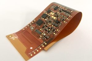
PCB material is also an essential factor that determines the quality of your PCB. There are various materials available for different types of PCBs. You need to select the suitable material according to your requirements. Some common types of materials are FR-4, Polyimide, Kapton, Rogers, etc. Here is a detailed criterion for choosing the suitable PCB material. For PCB prototype boards, the standard material is FR-4, and most companies only provide prototypes on FR-4.
PCB can be made in single, double, and multiple layers. The layers can be more than two dozen.
- Single-Layer PCB: A single-layer PCB has only one metal layer over the base material. This metallic coating is a conductor that provides electrical paths to components.
- Double-Layer PCB: A double-layer PCB has two layers of metals on different sides. It can also be called a two-sided PCB.
- Multilayer PCB: This type has three or more thin metal layers. The layers can be as many as possible and required. These are the complex PCBs.
The metallic layer that is used in PCBs is usually copper. Copper has high conductivity and good weldability. Therefore, it is mainly used. You can select the number of layers according to the types of PCB and your requirements. Usually, in PCB prototype services, the layers are fewer for faster delivery.
- Dimensions
You need to know about the dimensions and the size of your PCB. All PCB prototype manufacturers have a limited size. They have a specific maximum board size that they can make. So, calculate the size of your PCB and check which manufacturer can provide that size. The maximum size also differs according to the type of PCB. While designing a PCB, utilize every space and make a small PCB. The smaller the PCB, the lesser will be the cost.
Moreover, the regular shape in PCB manufacturing is a rectangle. So, if you select any irregular shape, there will be a waste of the board. You need to come up with a small size and available shape that requires less cost. No doubt that way does not matter much in a PCB prototype board because you only need a few PCBs, but it matters a lot in bulk manufacturing.
- Thickness
The thickness of the PCB is its width. It mainly depends on the number of layers you have selected. According to the type of PCB, there are different thickness ranges. You can discuss the thickness with your manufacturer. The thickness can be as small as 0.1mm and as large as 8mm or more.
- Spacing and Width
The conducting lines or traces on PCBs have a certain width. There is also spacing between two lines/traces. Every PCB manufacturer has a minimum limit of spacing and width. If the width and spacing are less, then the PCB will be compact. But it requires advanced technology and high cost to make a small PCB with very little spacing and width. At JHY PCB, we can provide a minimum diameter and tracing of 2.5 miles. You need to tell the spacing and width of values to your PCB manufacturer.
- Holes
There are via holes and drilling holes on PCBs. Both serve different purposes. There is a minimum hole diameter for different PCB types. You also need to see these values. There are various technologies for making these mechanical holes and lasers. Laser drilling is an advanced technology.
The solder mask is the polymer layer over the metallic layer of the PCB. This layer is essential, and it prevents the short-circuiting of adjacent traces. It also protects the copper under it. It is usually green, but most PCB manufacturers provide several colors for solder masks. You can select white, green, blue, black, red, yellow, etc. The color of the solder mask depends on your requirements.
To improve the solderability of copper, another metallic finish is applied, known as the surface finish. Different plating techniques include HASL (Hot Air Solder Leveling), HASL Lead-free, flash gold, ENIG (Electroless Nickel Immersion Gold), Immersion Tin, Immersion Silver, etc. You can select the most feasible one for your prototype. The benefit of the surface finish is that it protects the copper from oxidation.
- Copper Thickness
The thickness of the copper layer can also be customized. You can ask the PCB manufacturing company about it. It is measured in ounces. It can be 1oz, 2oz, etc. The thickness can be less than 1oz and more than 30oz. You need to choose the thickness according to your project.
- Silkscreen
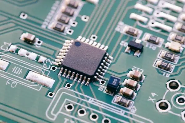
You might have seen printing on PCBs. This printing is known as silkscreen. You can select the color of the silkscreen as you like. The standard colors are white, black, and yellow. The printing should be clear so that the user can see everything easily. The PCB prototype board will give you a complete idea of printing quality.

