PCB Fabrication Process Flow Chart
What are the PCB manufacturing process steps?
How to build a multilayer and double-sided printed circuit board?
25 steps to manufacture a printed circuit board.
PCB, or printed circuit board, is an important electronic part and the support body of electronic components. Because it is made by electronic printing, it is called “printed” circuit board.
Electronic products in the production process, there will be a printed circuit board production process. Printed circuit boards are used in electronic products in all industries. It is an electronic schematic diagram can realize the design function of the carrier, let the design into physical products.
PCB production is a highly professional and complex process. Not only involves advanced production equipment, advanced production process, but also needs professional engineering and technical personnel and an excellent production management system.
As it happens, JHYPCB is just the professional PCB manufacturer you need.
Are you ready to get a quote?
Circuit Board Manufacturing Process
Why do we need to understand the PCB manufacturing process?
Some peers in the electronic manufacturing services industry do not think it is necessary to understand the entire process of PCB manufacturing. Even some PCB designers have the idea that the manufacturing process is not a design task but an outsourced task performed by the manufacturer. Remember, if you understand the complete PCB manufacturing process, you can properly choose the layout, trace parameters, types, materials, via hole locations, and other essential board aspects. Here are reasons to consider understanding the entire process.
Manufacturability
By understanding the PCB manufacturing process, you can determine the manufacturability of a design. These encompass maintaining enough space between the circuit board's edge and surface elements.
Cost Factor
Cost is always one of the factors we need to consider. Understanding the PCB manufacturing process can guide and improve our PCB design, ultimately achieving cost savings.
Quality Control
Understanding the steps and details of the PCB manufacturing process can effectively help us control the quality of the printed circuit board to ensure product yield.
What is the structure of the PCB board?
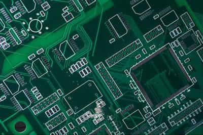
There are four parts to a printed circuit board:
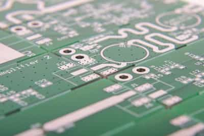
- Substrate: It is usually FR-4, which is made of fiberglass, the “skeleton of the PCB.” Fiberglass provides core strength to the printed circuit board and helps resist breakage.
- Copper Layer: Depending on the board type, this layer can either be copper foil or a full-on copper coating. The copper layer’s function is to carry electrical signals to and from the PCB like your nervous system carries signals between your brain and muscles.
- Solder Mask: The solder mask is a layer of polymer that helps protect the bare copper so that it doesn’t short-circuit from coming into contact with the environment. The solder mask acts as the PCB’s “skin.”
- Silkscreen: The silkscreen is usually on the component side of the PCB board and is used to show part numbers, logos, symbols switch settings, component references, and test points. The silkscreen can also be known as legend or nomenclature.
Printed Circuit Board Fabrication Process
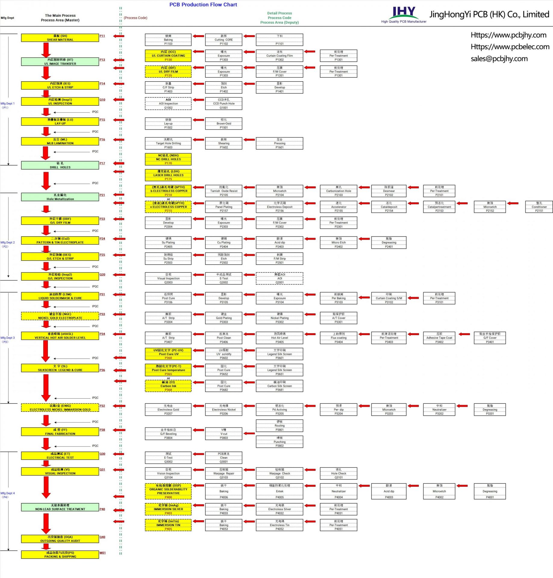
PCB Fabrication Process Flow Chart
Click on the image to view a larger image or download it.
Detailed schematic diagram of PCB manufacturing process
The following is an example of the production of a typical multi-layer PCB circuit board.
Table of contents
- Step 2: Multilayer PCB inner layer manufacturing process
- Step 2.1: PCB Materials and Cut Laminate
- Step 2.2: Inner Layer Image Transfer-Paste Film
- Step 2.3: Inner layer image transfer—Exposure
- Step 2.4: Inner layer image transfer—Developing
- Step 2.5: Inner layer image transfer—Etching
- Step 2.6: Inner layer image transfer—Stripping
- Step 2.7: Laminating-Stack up
- Step 2.8: Laminating - Lamination
- Step 2.9: Drilling
- Step 2.10: PTH(Plate Through Hole)
- Step 3: Multilayer Printed Circuit Board Outer-layer Manufacturing Process
- Step 3.1: Outer-layer Image Transfer - Paste Film
- Step 3.2: Outer Layer Image Transfer—Exposure
- Step 3.3: Outer Layer Image Transfer—Developing
- Step 3.4: Pattern Plating-Copper plating+Tin plating
- Step 3.5: Outer Layer Etching-Stripping
- Step 3.6: Outer Layer Etching-Etching
- Step 3.7: Outer Layer Etching-Tin Stripping
- Step 3.8: Solder Mask
- Step 3.9: Surface Finish
1, Preparation and process before PCB production
The PCB pre-production stage is a critical phase in PCB manufacturing that involves several important tasks, such as PCB design review, production parameter determination, manufacturing technology selection, production process development, production equipment preparation, quality control implementation, and customer communication establishment. By carefully planning, controlling, and supervising these tasks during the pre-production stage, high-quality, reliable, specification-compliant, and customer-oriented PCB products can be manufactured.
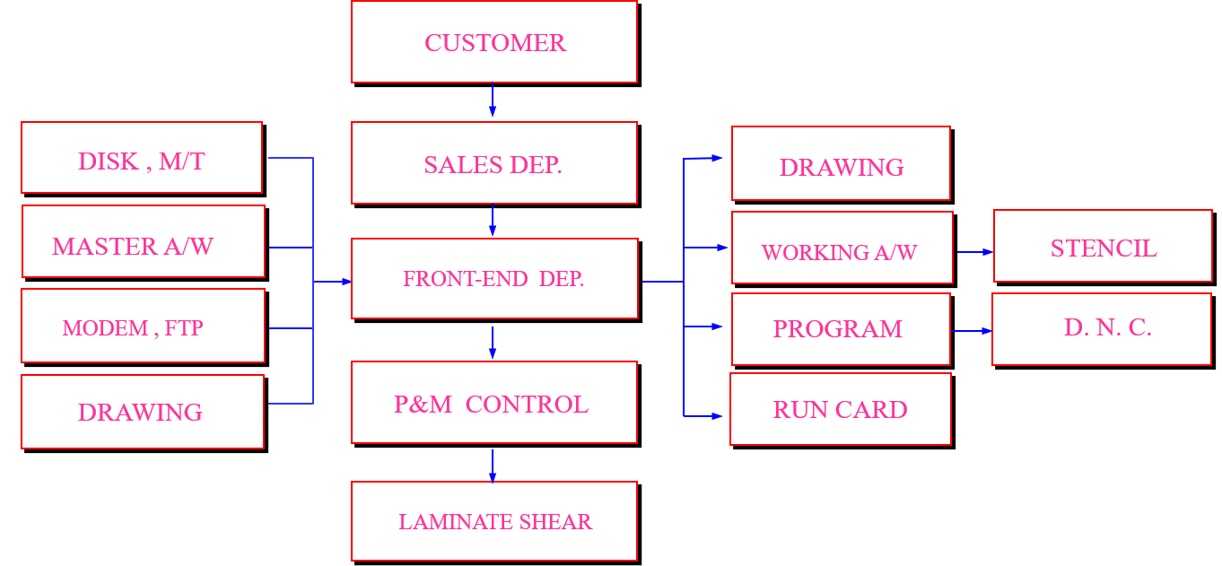
2, Multilayer PCB inner layer manufacturing process
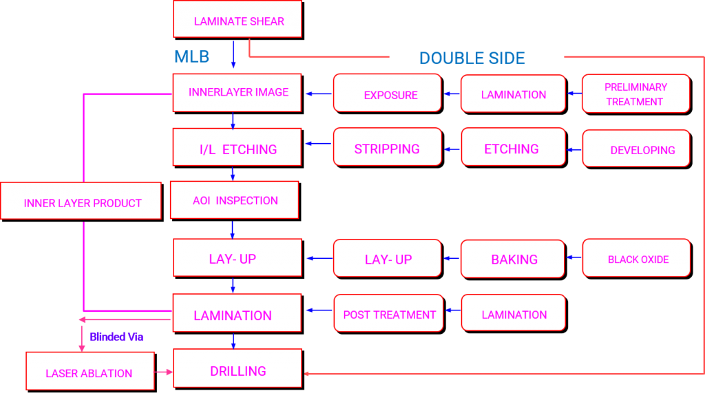
The manufacturing process for multilayer PCB inner layers involves several important steps. First, the inner layer cores are produced by cutting and drilling thin laminated sheets of copper-clad laminate material to the desired size and shape. The inner layer cores are then cleaned and coated with a photosensitive material. A film is then applied to the photosensitive material, and the design is printed onto the film using a laser or other imaging tool. The printed film is then placed onto the photosensitive material, and the entire structure is exposed to UV light. After exposure, the film is removed, and the unexposed areas of the photosensitive material are chemically removed. The exposed copper is then etched away, leaving only the copper traces and pads. The process is repeated for each layer of the PCB, and the inner layers are then laminated together under heat and pressure. Finally, the laminated stack is drilled and plated to create the vias that connect the layers of the multilayer PCB.
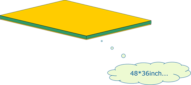
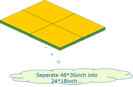
PCB manufacturing commences with a large sheet of material, which must conform to the factory’s equipment and processing capabilities regarding minimum and maximum size requirements. To comply with the manufacturing instructions (MI), the raw material for PCBs, known as Copper Clad Laminate (CCL), is automatically cut to the processing size using a cutting machine prior to production.
Inner Layer Image Transfer
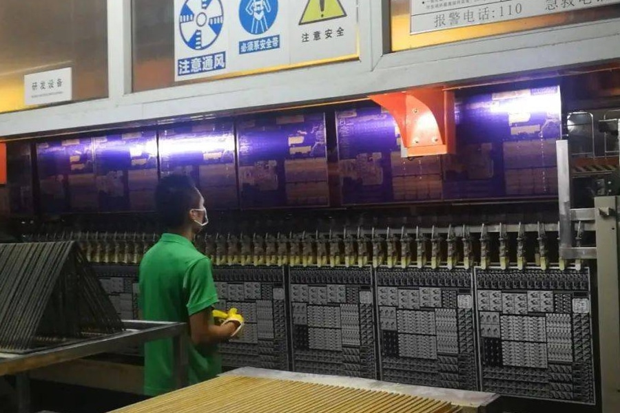
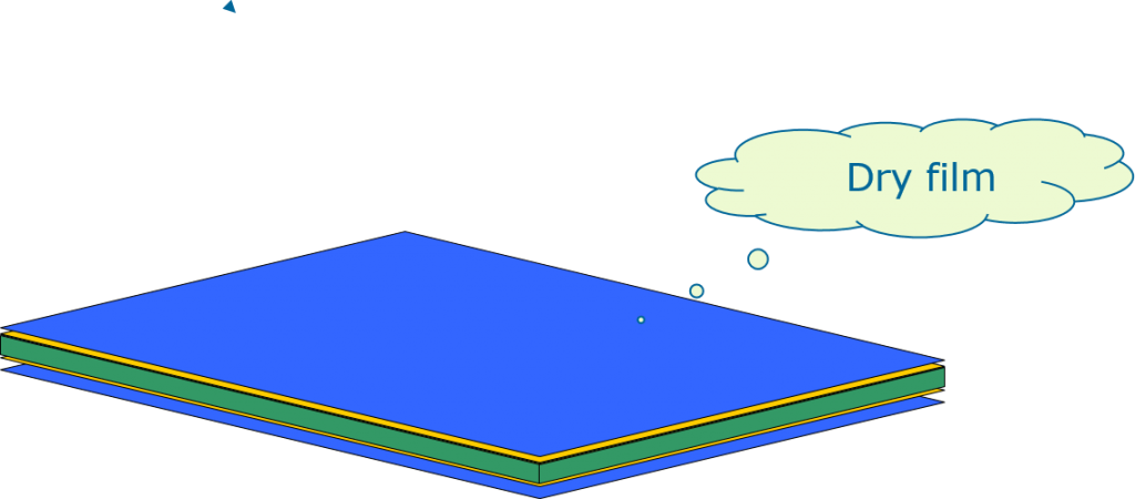
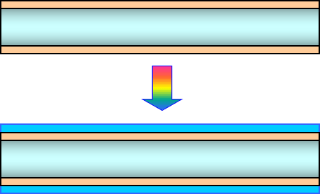
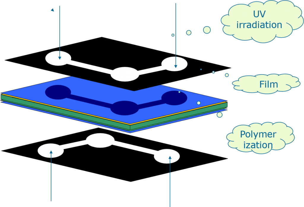
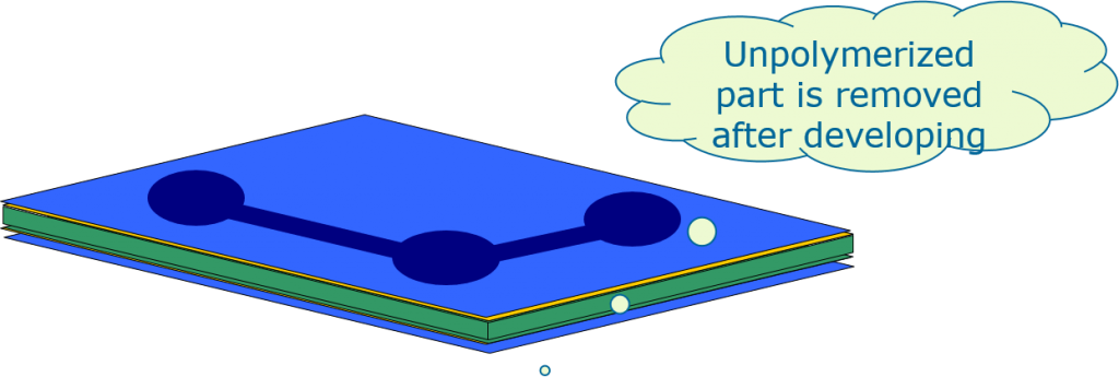
The inner layer image transfer process in multilayer PCB manufacturing involves several steps. First, a dry film is laminated onto the inner layer copper surface using a lamination machine. The dry film is then exposed to UV light through a photomask, which selectively hardens the film in the areas where the circuit pattern is present. The unexposed areas remain soft and are removed in a developer solution, leaving the circuit pattern on the copper surface.
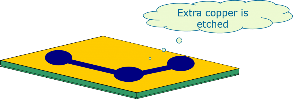
Next, an etching solution is used to remove the exposed copper, leaving the circuit pattern on the inner layer. The dry film is then removed with a stripping solution, leaving the copper circuit pattern behind.
After the inner layer circuit pattern is formed, the layer is cleaned to prepare for the next step in the multilayer PCB manufacturing process. The inner layer is then laminated with prepreg, and the process is repeated for the remaining inner layers. Once all inner layers are completed, they are stacked and laminated together with outer layers to form the final multilayer PCB.
2.2, Inner Layer Image Transfer-Paste Film
2.3, Inner layer image transfer—Exposure

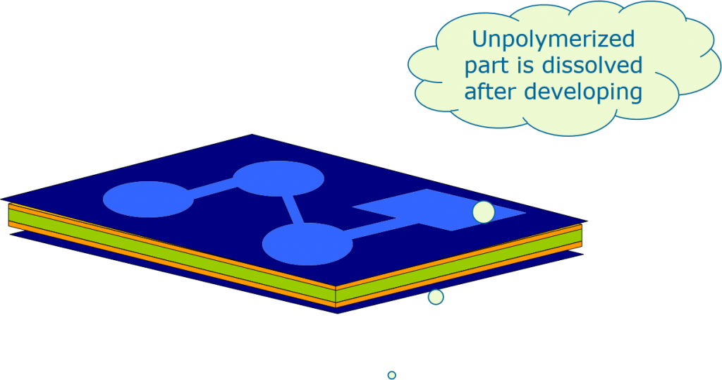
2.4, Inner layer image transfer—Developing

2.5, Inner layer image transfer—Etching
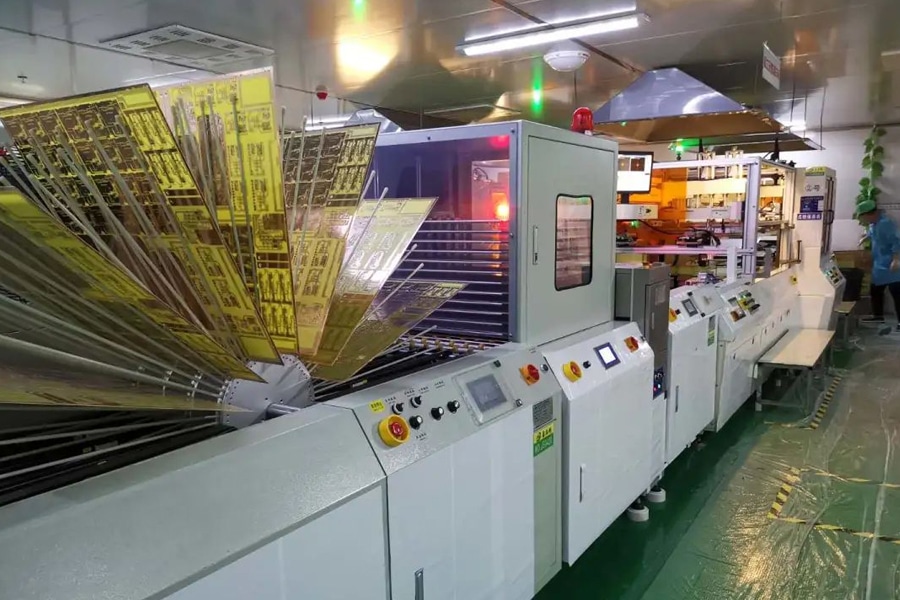
The process involves removing excess copper from the board by etching. The portions of the board covered by light ink have hardened and protect the copper underneath, which remains on the board after etching.
After etching, the board undergoes an alkaline wash to remove any unhardened resist. The technician then dips the board into a copper solvent to remove the exposed copper from the non-conductive areas.

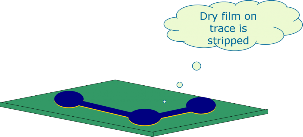
2.6, Inner layer image transfer—Stripping
Resist stripping is a process of removing any residual resist on the copper of the inner layer of a PCB. This is important to prevent any interference with the copper, which can affect its conductivity. Once this step is completed, the manufacturer can inspect the basic design of the PCB layer.

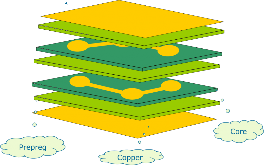
2.7, Laminating-Stack up
During the layup process, a computer-controlled machine is utilized to precisely align, heat and bond the layers of a multilayer PCB together with an insulating material and a copper foil layer sandwiched between the inner and outer layers. This is necessary to ensure the formation of a flawless structure for the printed circuit board, hence the reliance on computer-guided machines.
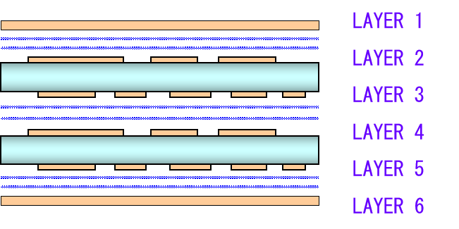
2.8, Laminating - Lamination
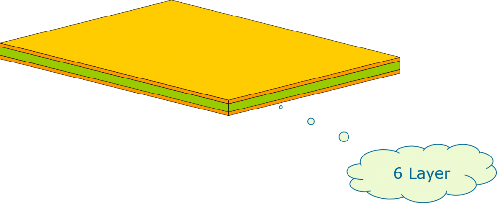
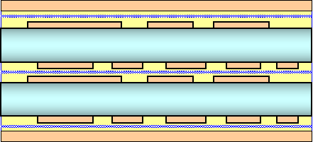
The lamination process involves the application of heat and pressure to dissolve the bonding epoxy between the layers of the PCB. When done correctly, this results in tightly held layers with effective insulation between them.
2.9, Drilling
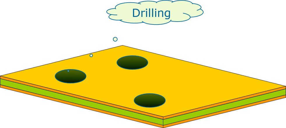
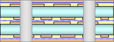
Prior to commencing drilling, the drill spots are precisely located using an X-ray machine. Following this, registration holes are drilled to secure the PCB stack-up in position before drilling the intended holes. The drilling is performed by a computer-guided machine using the Extended Gerber design file as a reference to expose the substrate and inner panels. Once the drilling is complete, any remaining copper is removed.
The holes created during this process facilitate the electrical connections within the multilayer PCB. To ensure proper registration to all inner layer connections, the mechanical drilling process must be optimized. This process allows for the stacking of the panels. Laser drilling is also an alternative method for drilling.
2.10, PTH(Plate Through Hole)
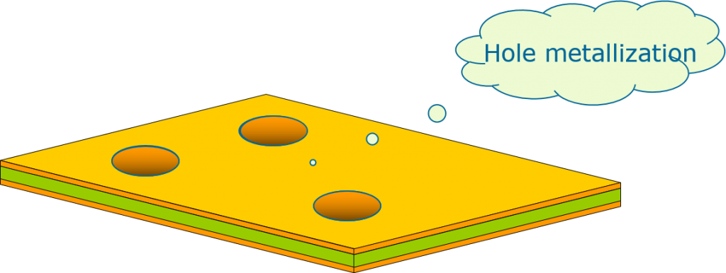
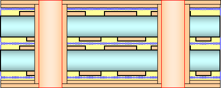
The initial stage of the plating process involves chemically depositing a very thin layer of copper on the walls of the holes. This process, known as PTH, results in a thin layer of copper covering both the hole wall and the entire panel. It is a complex chemical process that requires strict control to ensure a reliable deposition of copper, even on non-metallic hole walls. Although the amount of copper deposited at this stage is not sufficient on its own, it provides electrical continuity between layers and through the holes.
Following PTH, panel plating is carried out to create a thicker layer of copper on top of the PTH deposit, usually ranging from 5 to 8 um. This combination of PTH and panel plating is optimized to achieve the required track and gap demands by controlling the amount of copper to be plated and etched.
3, Multilayer Printed Circuit Board Outer-layer Manufacturing Process
The outer layer production process for multilayer PCBs:
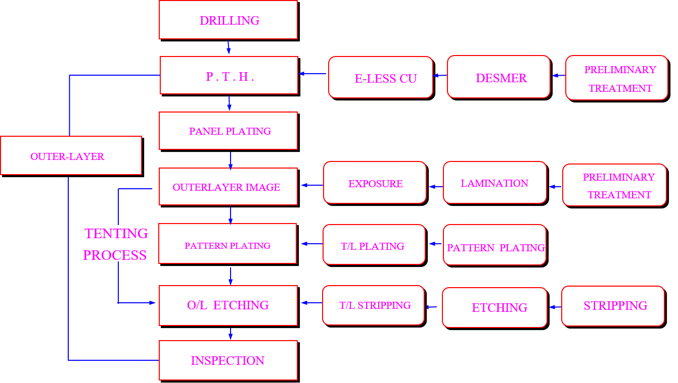
Outer layer imaging: A photosensitive coating is applied to the copper foil, and the coating is exposed using photolithography to define the pattern of the required circuitry and components. The exposed copper is then removed by chemical etching or plating, leaving behind the required circuitry.
Pad fabrication: Copper is either electroplated or chemically deposited on the entire surface of the PCB, then exposed using photolithography to define the required pad pattern. Finally, metal is plated onto the exposed areas to create the required pads.
Solder mask application: A protective coating is applied to the surface of the PCB to protect it from corrosion and environmental damage. This is typically achieved through spray or immersion coating that covers the entire surface of the PCB.
Silk screening: To facilitate identification of different components and pins, letters and numbers are printed on the surface of the PCB. This is typically achieved through screen printing or inkjet printing.
Inspection and testing: The final step is to inspect and test the outer layer to ensure the quality and reliability of the PCB. This is typically done through visual inspection, X-ray inspection, and electrical testing.
Outer Layer Image
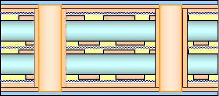
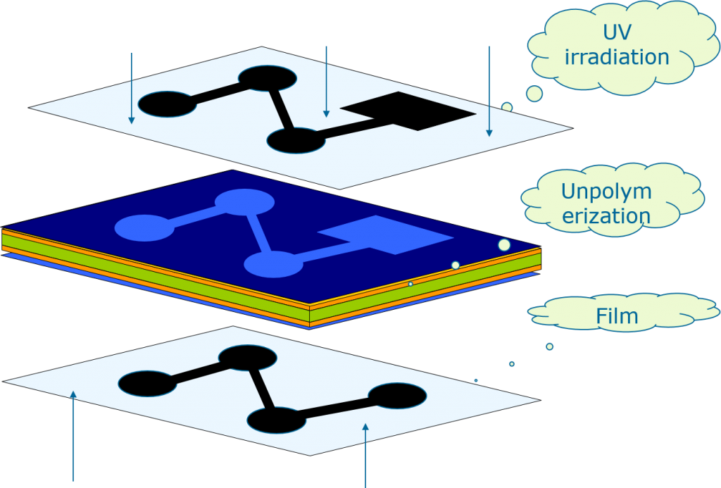
The outer layer process follows a similar procedure to the inner layer process, which involves transferring an image using photosensitive dry film, exposing it to UV light, and then etching it. However, the key difference is that during the outer layer process, the dry film is removed only where copper needs to be preserved or where circuitry is to be defined, allowing for additional copper to be plated in subsequent steps of the process. This process is typically performed in a clean room environment.
3.1, Outer-layer Image Transfer - Paste Film

3.2, Outer Layer Image Transfer—Exposure
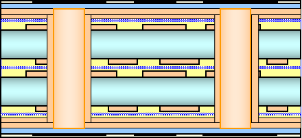
3.3, Outer Layer Image Transfer—Developing
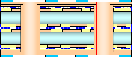
3.4, Pattern Plating-Copper plating+Tin plating
In the second stage of electrolytic plating, the plating process occurs in regions where there is no dry film or circuitry. After the copper plating is complete, a layer of tin is added to safeguard the newly plated copper.

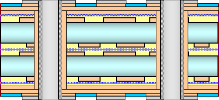
3.5, Outer Layer Etching-Stripping
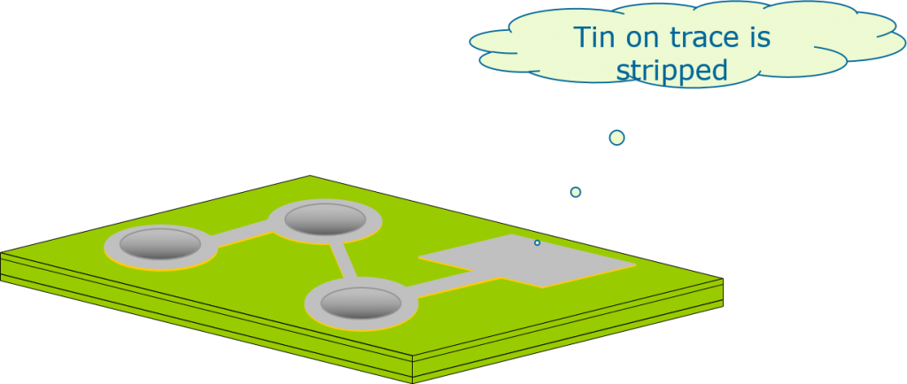
Typically, outer layer etching process involves three steps. The initial step involves eliminating the blue dry film, followed by etching away the unwanted copper, while using the tin deposit as an etch resist to preserve the required copper. Finally, the third and last step is to chemically eliminate the tin deposit, thereby revealing the circuitry.
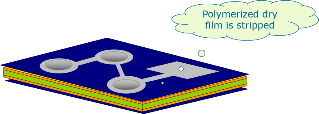
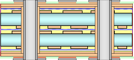
3.6, Outer Layer Etching-Etching
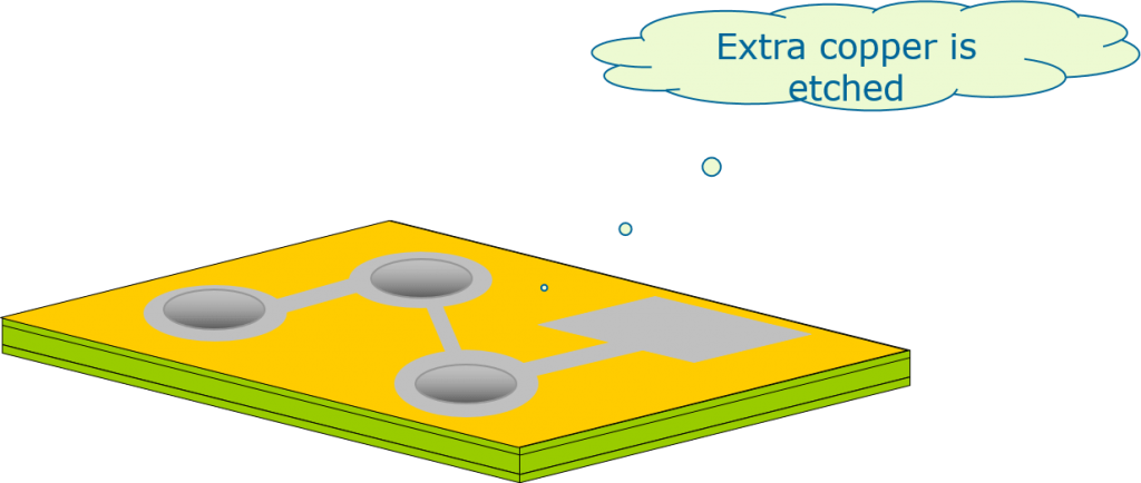
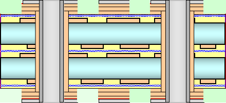
3.7, Outer Layer Etching-Tin Stripping
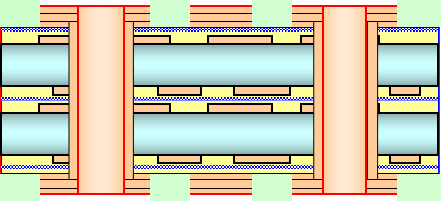
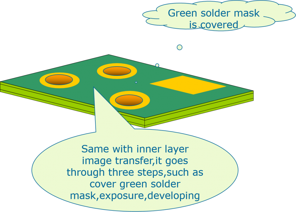
The entire surface of the PCB is coated with soldermask ink. Through the use of artworks and UV light, specific areas are exposed to UV, while the unexposed regions are eliminated during the chemical development stage. Typically, the areas that are to be utilized as solderable surfaces are the ones that remain. The residual soldermask is then completely cured, creating a durable finish. This process is carried out in a sterile environment, known as a clean room.
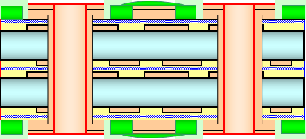
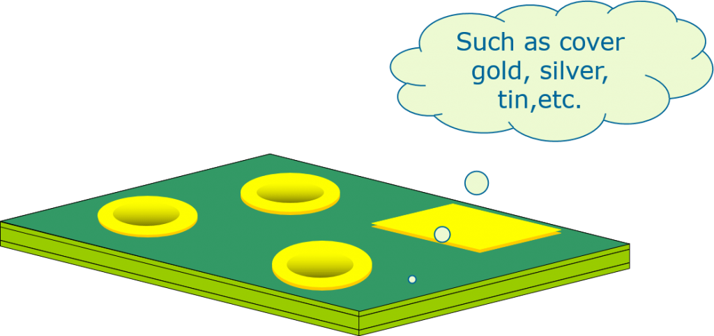
The exposed copper areas are treated with different coatings to safeguard the surface and ensure excellent solderability. The coatings may include Electroless Nickel Immersion Gold, HASL, Immersion Silver, among others. The thickness of the coatings and their solderability are always tested and assessed.
The surface treatment process includes OSP|HASL|HASL Lead-Free (HASL LF)|Immersion Silver|Immersion Tin|Plated Gold|Immersion Gold(ENIG)|ENEPIG|Golden Finger+HASL|ENIG+OSP|ENIG+Golden Finger|OSP+Golden Finger, etc.
4, External View and Molding Process Flow Path
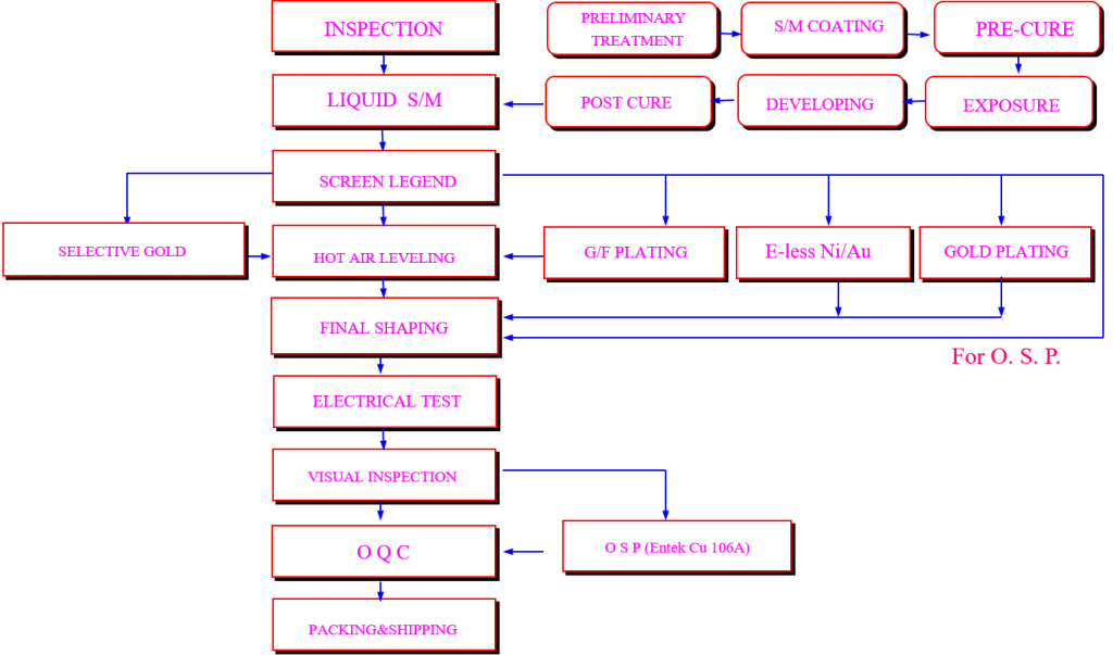
5, Summary
1) Inner Layer
> Chemical Clean
> Cut Sheet Dry Film Lamination
> Image Expose
> Image Develop
> Copper Etch
> Strip Resist
> Post Etch Punch
> AOI Inspection AOI
> Oxide
> Layup
> Vacuum Lamination Press
2) CNC Drilling
> CNC Drilling
3) Outer Layer
> Deburr
> Etch back – Desmear
> Electroless Copper
> Cut Sheet Dry Film Lamination
> Image Expose
> Image Develop
4) Plating
> Image Develop
> Copper Pattern Electro Plating
> Tin Pattern Electro Plating
> Strip Resist
> Copper Etch
> Strip Tin
5) Solder Mask
> Surface prep
> LPI coating side 1
> Tack Dry
> LPI coating side 2
> Tack Dry
> Image Expose
> Image Develop
> Thermal Cure Soldermask
6) Surface finish
> HASL, Silver, OSP, ENIG, etc.
> Tab Gold if any
> Legend
7) Profile
> NC Routing or punch
8) ET Testing, continuity and isolation
9) QC Inspection
> Ionics
> 100% Visual Inspection
> Audit Sample Mechanical Inspection
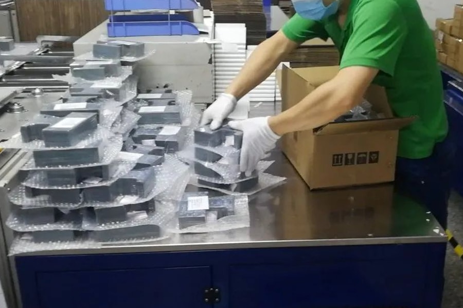
> Pack & Shipping
A super detailed step-by-step guide to the PCB manufacturing process
Recommended PCB Manufacturing Services
Related Posts
- How to Build a Multilayer PCB?
- Electronic PCB Assembly Process and Flow Chart
- Guide to Multilayer PCB Layer Stackup and thickness
- Knowledge of Plating on Flexible Circuit Board Surface
- Knowledge of Flexible Printed Circuit Board Processing Technology
- The terms you have to know related to the manufacture of Flexible PCB
- Unveil the mystery of high TG PCB circuit boards Materials
- Why choose FR4 as the general material of PCB?
- Why is FR4 Used to Make High Tg PCBs?
- PCB and PCBA Manufacturing Files
- Double-sided PCB Manufacturing Process
- How to Store PCB and PCBA?
