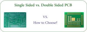
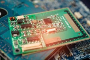
When designing PCBs, engineers must make thoughtful layout and component placement decisions that consider both functionality and manufacturability of their boards. One key choice is whether to design a single-sided or double-sided PCB.
While simpler and cheaper, single-sided boards severely limit the complexity and optimization of a layout. In contrast, double-sided PCB construction opens doors for more creative and capable designs.
In this blog post, we’ll explain four key advantages of using a double-sided PCB over their single-sided counterparts:
- More layout space for traces and components
- Ability to achieve complex circuit designs with just two layers
- Improved signal integrity for critical paths
- Flexible layout arrangements to keep connected components close
For hardware developers producing prototype designs, double-layer boards unlock critical capabilities. The rest of this article will expand on the core benefits listed above and demonstrate why opting for two-layer construction sets creators up for prototyping success. We’ll also touch on partnering with quality suppliers like JHYPCB capable of delivering affordable yet high-performance double-sided boards with expedited assembly in low volumes.
Table of Contents
More Available Space Enables Complex Layouts
The most straightforward advantage of double-sided boards is the increased real estate for placing traces, routing signals between components, and hosting the elements themselves.
With a single copper layer, circuit designers face strict limitations aligning components while still leaving adequate spacing for traces. This confinement heavily restricts overall complexity, connections, and creativity in laying out the schematic. Engineers frequently have to compromise optimized placement to make a single layer work.
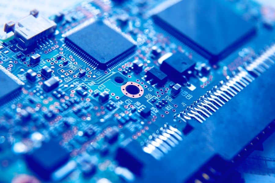
Adding a second conductive layer flips this problem on its head. Now both sides of the substrate contain viable area for hosting ICs, discretes passives, necessary text markings, copper fills, vias, and of course etching conductors between everything. This layout flexibility unlocks far more intricate architectures comprising greater component counts and node densities.
In essence, rather than piecing together a jigsaw puzzle on a wall, the double-sided board serves as a worktable allowing components placement for cleaner interconnectivity. The second layer affords the simplicity of necessary crisscrossing traces rather than pick between collide prone diagonal sideways routing or extending trace lengths suboptimally. This extra dimension available means ability to emulate finer node ICs at larger geometric scales. And subsequently reduced risks of fault or failure.
In short, added layout space relieves the allocation pressures of single-layer attempts. With diligent planning, vastly more capable prototyping blueprints come to fruition using the enviable versatility 2 layer PCBs offer.
Achieve Complex Circuits with Just Two Layers
Another main advantage of double sided boards is enabling more complicated circuit topologies while minimizing overall board layer counts. This directly benefits prototyping applications where cost and turnaround time take priority.
Consider functional blocks like a microcontroller, power regulation, supporting ICs, crystal oscillators, decoupling capacitors, peripherals, and external interfaces. Cramming all these subcircuits onto a single layer demands intense optimization and forces many compromises. Routing tends to suffer from haphazard patchworks struggling to connect distant components.
Transitioning these same design goals to a dual-layer board alleviates tremendous burdens. The extra dimension permits careful floor planning to position connected elements closer together right from the start intentionally. With convenient access between top and bottom layers via plated-through holes, traces follow more sensible paths. Components critical for high-frequency operation can readily locate adjacent to one another as well.
For developers aiming to test ambitious theory in physical form, double sided boards enable achieving remarkable circuit complexity from just 2 conductive foils. This means reducing layer count compared to 4, 6, or more layer single-face alternatives. In turn lowering costs and build times to start evaluating functional prototypes sooner.

Improved Signal Integrity
A third compelling reason to select double sided PCBs is attaining better signal integrity, especially for time sensitive analog or high speed digital signals.
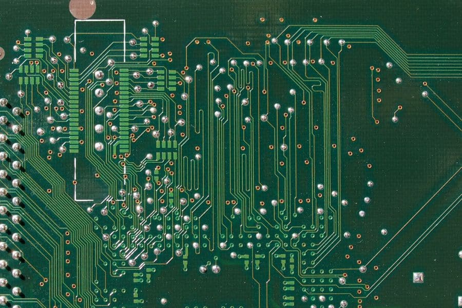
Length correlates strongly with parasitic resistance and capacitance when tracing a conductive path between two components. Longer traces increase these parasitic, allowing greater opportunity for interference coupling from nearby signals. Effect severity scales exponentially as operating frequencies, edge rates, and resolution requirements increase.
Double-sided construction mitigates such signal degradation by reducing trace lengths and inserting ground planes. Sensitive pathways can follow more direct A-to-B routes between top and bottom layers rather than meandering single-face detours. With a whole second layer, planes are divided amongst power delivery, grounding, and shielding instead of one layer pulls triple duty.
This advantage manifests clearly for circuits like a radio tuner pathway must remain untouched from amplifier noise contamination. Or when a MCU relies on clean clock waveforms within nanosecond edge rates. Tucking these traces in close proximity with intentions of isolation bolsters integrity. Dual layer boards thus foster and protect delicate signals by affording shorter traverses alongside intentional partitioning amongst referencing planes.
For quick yet functional prototyping applications, having robust signals enduring noise promises much greater early testing success and insights towards perfection down the road. Double-sided PCBs better deliver on that promise.
Flexible Layouts and Component Placement
The final principle benefit double-sided PCBs provide is dramatically increased flexibility when arranging components and routing traces. This layout versatility facilitates creative solutions to achieve designs otherwise challenging or unfeasible with single-layered boards.
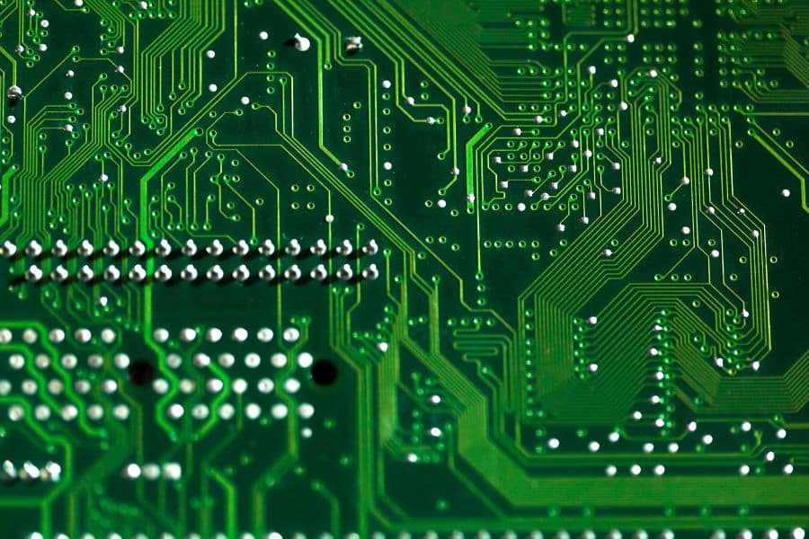
With dual foils, engineers enjoy extensive options placing ICs, discretes, connectors first then stitching together with interconnects. Related functional blocks get positioned intentionally close rather than distant due to lack of room. Critical nets can daisy chain on one layer to avoid obstruction. Decoupling caps mount right at supply pins without complex snaking trails.
In essence, doubling available real estate opens up a multidimensional canvas for circuit architects to sketch artwork circuit maps. The second layer erases constraints of channeling all intricacies along a single plane. Automatic routing algorithms converge quicker while manual layouts breathe simpler. Density and complexity skyrockets giving way to capable prototyping platforms.
Of course, refined layout skills and sound design principles still reign importance over randomly scattering components then struggling to wire the mess through either board face. But for those who embrace conscientious planning, dual layer PCBs empower remarkable flexibility to organize, arrange and connect innovative circuit ideas once restricted as purely theoretical. This flexibility accelerates design iterations and proof of concept validation – two cornerstones of successful rapid prototyping.
Double Sided Boards Unlock Prototyping Potential
When combined, the major benefits of additional layout space, reduced layers for complexity, superior signal integrity and flexible component placement paint a compelling picture for choosing double-sided PCBs. This is especially true when designing for prototyping applications rather than high-volume production.
The dual-layer approach unlocks the potential for testing innovative circuits rapidly without requiring as much upfront time, cost, and optimization. Engineers gain more creative freedom by arranging their designs in a manner that verifies functionality first while optimizing manufacturability later.
In short, double-sided PCB construction strikes an ideal balance of affordability, lead time, and performance for elevating a prototype from concept to physical validation.
Here at JHYPCB, we specialize in delivering affordable yet high-quality double-layered boards on aggressive lead times. Our capabilities not only include precision board fabrication, but also assembly of components onto supplied prints. So whether you need unpopulated boards or full SMT mounting, we have solutions tailored for prototyping digital circuits, analog sensors, wireless communicators, power controllers, and more. Contact us to learn how our passion for PCBs can accelerate your next electronic design.
Related Reading
The Benefits of Using Double Sided PCBs