Design For Manufacturing (DFM) studies the relationship between the physical (mechanical and electrical) model of the product itself and the manufacturing and processing system. It incorporates it in product design to integrate it with the requirements of the entire manufacturing system. It makes the designed product easy to manufacture, reduces quality defects in the manufacturing process, shortens product development or production cycles, reduces costs, and improves outcomes. The purpose is to achieve quality and production efficiency. The manufacturability of a product should include the feasibility of the whole process of product manufacturing, testing, rework, and repair. Still, in a narrow sense, it refers to the usefulness of the product itself.
PCB Design for Manufacturability
PCB is the basis of electronic products, and the designed PCB graphics should be used for both PCB manufacturing and PCB assembly. The PCB manufacturing and the PCB assembly belong to two different manufacturing professions. The two are very different in manufacturing process methods and equipment, and manufacturing requirements are also very different. Therefore, the designed PCB needs to meet two manufacturability requirements at the same time: its manufacturability requirements and the manufacturability requirements of printed circuit board assemblies.
PCB design, manufacturing, and assembly belong to three different professional technical fields. As an excellent PCB designer, you must be proficient in circuit design and understand and be familiar with PCB manufacturing and component installation process requirements. It would help if you even understood the characteristics and essential dimensions of the selected components and the installation and welding. The elements of the features of the solder and flux must be integrated organically. Achieving overall optimization in design is not an easy task, which requires a wealth of practical design experience.
The PCB DFM includes the manufacturability of the PCB itself and the manufacturability of printed circuit board assembly. The manufacturability of the PCB itself needs to consider the requirements of the printed board production process specification. The manufacturability of the printed board assembly needs to discuss the assembly process specification requirements.
For the Design For Manufacturing of the PCB itself, the primary consideration is the PCB design requirements of the printed circuit board manufacturing process. There are many PCBs (such as multilayer rigid circuit boards and single-sided or double-sided PCBs). Different models have different processing methods, and their manufacturability design requirements are different. When designing the PCB, it is necessary to understand the characteristics of the relevant PCB production process and consider the design of manufacturability according to the structural features of the designed PCB.
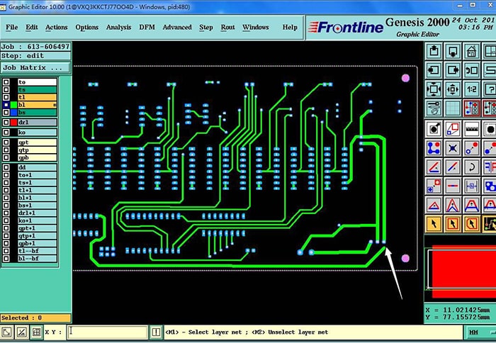
The technical indicators required for the manufacturability of PCB are related to the development status of PCB manufacturing process technology and the printed board manufacturer. For example, a PCB with a wire width of 0.1mm and a minimum through-hole diameter of 0.3mm cannot be processed by all manufacturers. Only some factories with better equipment and technological conditions can process it. Some designers do not pay attention to these problems, thinking that products can be manufactured after they are designed or whether the layout and wiring design of the printed circuit board are correct is their own business. They also think that manufacturing is a matter of production and craftsmanship. This concept is wrong. When considering the technical indicators of PCB manufacturability, it should be determined according to the current printed board processing technology level and the printed board manufacturer’s process requirements that are expected to be selected; otherwise, the designed product will be challenging impossible to make.
Design Factors
Some of the design factors that need to be considered to meet the manufacturability requirements of the PCB itself are as follows.
- The outline size and accuracy of the PCB are essential. Restricted by equipment processing size and accuracy requirements, the maximum and minimum processing size, dimensional accuracy, and the size of the process edge should be considered when designing.
- It would be best if you were careful in selecting PCB substrate types and specifications. The processing method of the printed board should be considered, and the type and size of the PCB substrate chosen should meet the standard as far as possible.
- Determine the structure and thickness of the PCB. The structure and consistency of the PCB must meet the electrical and mechanical requirements of the printed board, but the possibility of manufacturing must also be considered. For example, the maximum number of layers of a multilayer printed board, the total thickness of the intermediate dielectric layer and the board, etc., are all restricted by the production and processing capabilities. When determining these parameters, you should negotiate with the PCB manufacturer.
- Determine the ratio of PCB thickness to aperture. The ratio of the PCB thickness to the via is a vital index that restricts manufacturability. Restricted by the metallization hole process, the smaller the hole diameter and the thicker the substrate, the more complex the hole metallization is. Therefore, an appropriate plate thickness to hole diameter ratio should be selected to facilitate hole metallization and electroplating.
- Determine the minimum hole diameter and the minimum distance between holes. Restricted by the production equipment and hole metallization ability, the design should be considered compatible with the production capacity and level.
- Pay attention to the form of the land pattern. Since the minimum connecting pad width will be limited by PCB installation, soldering requirements, and printed board production accuracy, the manufacturability requirements of these two aspects should be comprehensively considered when designing.
- Pay attention to the width of printed wires, wire spacing, and accuracy. Restricted by the pattern transfer and etching process level in the production of the printed board, the production process will affect the withstand voltage between the printed board wires. The insulation resistance, the characteristic impedance of the printed board, and the design should be considered comprehensively.
- Design elements such as layout and wiring directly affect the installation of electronic components, printed board manufacturing accuracy, withstand voltage and insulation resistance, and the electromagnetic compatibility of the printed board. The uniformity of the wiring will also affect the mechanical properties, such as the warpage of the printed board, and then affect the reliability of the soldering of surface-mounted components. The process requirements and electrical requirements should consider the design.
- There are also some special manufacturability considerations for different PCBs, such as flexible printed boards and high-density interconnect boards.
Essential Considerations for Design for Assembly(DFA)
When considering the manufacturability design index of the PCB itself, it should not exceed the current manufacturing process limit of the PCB or the production capacity limit of the pre-selected manufacturer. If necessary, process negotiation with the pre-selected PCB manufacturer or production capacity of the manufacturer should be conducted. You can look at the certification to confirm qualified PCB manufacturers.
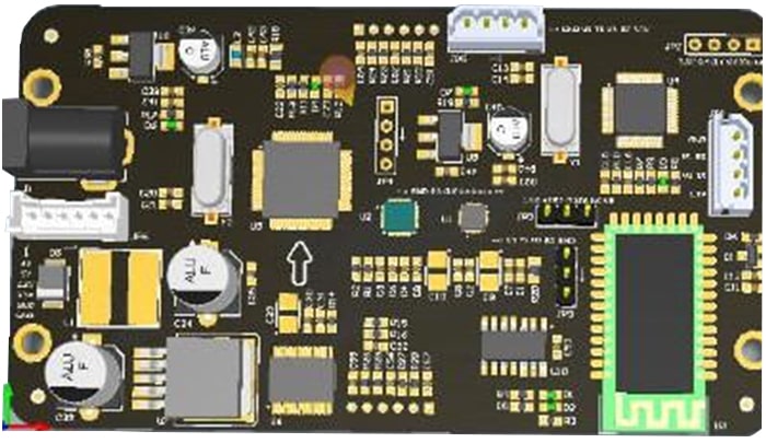
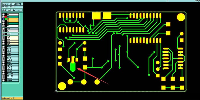
The Design for PCB assembly is determined when the PCB graphic design is completed. The installation of the components, the welding form, and the difficulty of product testing and maintenance are determined. So, for the manufacturability of the printed board assembly, the design must be considered in the graphic design of the printed circuit board. Because in the PCB graphic design, the installation position and density of the components and the wiring relationship of the connection during layout and wiring play a decisive role in whether the parts are installed correctly and whether they can be easily detected and repaired. Therefore, for PCB graphic design, the manufacturability of product installation, welding, maintenance, and testing should be considered.
The manufacturability design of the printed circuit board assembly varies significantly with the different installation methods of the components. According to the packaging form of the components, the mounting process of the printed circuit board can be divided into the through-hole mounting, surface mounting, micro-assembly, or direct chip packaging. Different installation methods have different requirements for the substrate and complexity of the printed board, so the design and manufacturability requirements for the printed board are also different.
The manufacturability design of the printed board assembly is also related to the way the components are soldered. The commonly used soldering methods include manual soldering, wave soldering, reflow soldering (reflow soldering), and pressure soldering (bonding). For manual soldering, the solder mask can be used or not. In wave soldering and reflow soldering, to prevent bridging and short circuits during soldering, a solder mask must be used. For reflow soldering in the middle, designing a template for screen printing solder paste is also necessary. When using the pressure welding connection, the matching problem of the coating (plating) layer on the pad’s surface should be considered. Different welding methods have different requirements for the type and thickness of the coating, and improper matching will cause welding failure or defects.
Regardless of which mounting method or welding method is used, the general requirements for the manufacturability design of printed board assemblies are as follows.
Design Requirements for Manufacturability of Printed Circuit Board Assembly
- During layout, the installation spacing of components and the distance from the board’s edge should meet the installation, maintenance, and testing requirements.
- The mounting holes of the components (including pins) should have enough gaps for insertion and welding.
- The size of the pad and the minimum ring width should meet the requirements for a reliable connection after soldering.
- The size and position of the pad should meet the requirements of installation and soldering quality.
- For components that need to be reinforced or require an external radiator, leave space for reinforcement and installation of the radiator.
- According to the heat generation of the components, determine whether the components are mounted on the board, off the board, or with an external heat sink according to the thermal design requirements. The layout and arrangement direction of the components should be conducive to heat dissipation.
- The installation position and polarity mark of the components should be clear and accurate and should be consistent with the requirements of the electrical schematic diagram. The screen-printing mark should meet the screen printing process requirements.
- The through-holes under the component body and other holes that do not need to be soldered should be covered with the solder resist to prevent the solder from flowing onto the component body during soldering. Otherwise, it can damage the component or short-circuit the component body of the metal shell.
- No other components or vias are allowed to be laid within the specified range around super-large-scale parts or heating components.
- Try to set the test points on the printed board on the board’s edge or a place that is not easily blocked by other components to facilitate the test.
- In the layout of components, electromagnetic compatibility should be fully considered.
Advanced Learning:


