Introduction
Low cost and high output have always been the eternal pursuit of all companies. Through the Design For Manufacturability(DFM) of the printed circuit board, the design department and the production department can be effectively connected organically. The design, development, and production can be coordinated to unify the standards, realize production automation, and improve production efficiency.
With the continuous development of the electronics industry, higher requirements are put forward for printed circuit boards, especially the widely used SMD components and assembly and soldering processes, which requires designers to consider printed circuit boards throughout the design for manufacturability. Therefore, PCB designers must combine reality when developing new products and designs for manufacturability in all aspects of the entire PCB design stage.
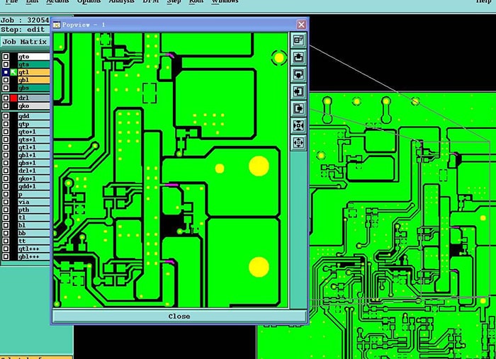
This article will analyze several factors that improve the design for the manufacturability of printed circuit boards from component selection, assembly methods, and component layout.
1. Selection of Components and Assembly Methods
Component selection mainly refers to more advantageous components in combination with selection, procurement, processing, and maintenance. The actual situation should determine the DFM selection of components within oneself and through consultation with purchasing engineers, hardware engineers, and process engineers.
The choice of assembly method and the component layout are essential aspects of PCB manufacturability, significantly impacting assembly efficiency, cost, and product quality. A better assembly method suitable for production can provide automated production efficiency and save more human resources and funds.
2. PCB Layout
PCB layout plays a key role in the entire PCB design. Product quality problems caused by poor structure are difficult to overcome in production. To correctly design layout as a whole to minimize welding defects and production losses, designers need to focus on the following factors when making layouts:
- The characters and graphic marks on the printed circuit board should be clear and unobstructed to provide practical guidance for later production.
- Leave a particular maintenance gap around the vulnerable components; do not place valuable components in the high-stress area of the printed circuit board, which will quickly cause cracks or cracks in the solder joints and components.
- The components are arranged in the same direction and polarity layout, which can increase the speed of insertion, and it is easy to find errors and improve production efficiency. The long axis of the passive component is perpendicular to the travel direction of the printed circuit board. The axial direction of the notch mark of the dual-row package component is parallel to the travel direction of the printed circuit board to prevent one end of the element from being heated. In contrast, the other end is displaced or raised.
- The power devices should be evenly placed on the edge of the PCB or the ventilation position in the chassis.
- Try not to place components on both sides of the printed circuit board, which will increase assembly labor and time. When there are components on both sides of the printed circuit board, for surface mount, place the most significant component on one side as much as possible. And evenly distributed, and the minor components are placed on the other side because the components are small, light, and the probability of separation is much lower than that of significant parts.
- Adjustable components should consider the structural requirements of the whole machine, and the layout of components should meet the needs of the production process.
- When adjusting the position of components, it is necessary to pay attention to the one-to-one correspondence between components and silkscreen symbols.
3. Other factors
The PCB Outline Size
The maximum width of the printed circuit board allowed for wave soldering is 250mm, and the total size of the printed circuit board required for reflow soldering is 330mmx250mm; it is designed with the golden section point 0.618. The physical size ratio of the printed circuit board is the best. In addition, the peripheral space requirements of the printed circuit board during the assembly of the whole machine, the location of the mounting hole, and the location of particular components should be considered comprehensively. To prevent the four corners of the printed circuit board from hurting people and facilitate mechanized production, rounding is done around the board frame, with a chamfering radius of 3mm to 5mm.
Positioning Holes
The installation positioning holes are generally designed on the board in advance to fix the printed circuit board conveniently. The positioning holes of the printed circuit board are non-porous (holes without metallization treatment, non-conductive). Design the hole diameter and position of the mounting holes according to the external environment of the printed circuit board installation. Please pay attention to the 1mm range of the mounting hole and its surroundings. Do not place components and wires inside to avoid short circuits with metal mounting screws.
Clamping Edges
The automation equipment used in the production requires automatic PCB transfer. In this way, a 3-5mm top clamping edge is needed on the upper and lower sides of the PCB to facilitate electronic transfer and avoid elements close to the board’s edge. The device cannot be automatically assembled due to clamping.
Location Marks
In the commonly used location marks, the two scores must be distributed on the diagonal of the PCB, and there should be an open area without other circuit features or marks around the mark. The size should preferably not be smaller than the diameter of the target. The score should not be located on the clamping edge of the printed circuit board, and the distance from the side of the board should be more than 5mm.
Besides, there should be corresponding positioning marks on the diagonal of PLCC components on the printed circuit board. The size and other requirements are the same as those on the printed circuit board.
PCB Thickness
The thickness of the PCB varies from 0.5mm to 4mm, and the depth of the commonly used PCB is 1.6mm and 2.0mm.
The thickness of the available PCB is 1.6mm; when the size of the board is large or one side is long, to prevent deformation and even fracture during processing, assembly, and welding, it is recommended to use a thickness of 2mm.
The Warpage of the PCB
If the printed circuit board is not flat, it will cause inaccurate positioning; components cannot be accurately inserted into the board’s component mounting holes and surface mount pads. Even the automatic plug-in installation will be damaged. If the board with the components is not flat, the mounting legs of the in-line components are difficult to cut neatly, and even the board cannot be installed in the chassis. Therefore, the warpage of printed circuit boards will cause a lot of trouble in production. Especially for surface-mounted printed circuit boards, the warpage must be less than 0.0075mm/mm.
Panelization
Panelize is divided into several types of boards or several forms of the same kind of board panelize, yin, yang panelize, and the mesh pattern of the stencil. The connection between the sub-boards can be a double-sided engraved V-groove, long slot, round hole, etc. To facilitate the final separation of the board, the design must consider making the separation line as straight as possible and think that the separation edge should not be too close to the PCB trace because the internal circuit of the PCB is easily damaged during the separation.
After the PCB board is assembled, the clamping edge must be considered for the effect of the whole board, and the sub-board with chip components must have positioning marks.
PCB Traces
The lines in the signal PCB cannot be set too thin to prevent excessive corrosion from causing the signal lines to be disconnected.
4. Summary
An excellent PCB designer must consider how to obtain good electrical performance and beautiful layout and find the design for manufacturability in PCB to achieve high quality, high efficiency, and low cost. With the unstoppable development trend of surface mount technology, electronic component products are getting smaller and smaller and more diversified, making more and more designs for manufacturability, and integrating into PCB design earlier and earlier. Suppose PCB designers apply the manufacturability ideas flexibly in the early stages of PCB design. In that case, the products will surely meet high quality, high efficiency, low cost, and best overall performance.
Advanced Learning:
- Basic Knowledge of PCB Pad Design
- PCB Terminology Glossary
- PCB Design Software Free Download
- What are the aspects of PCB Design For Manufacturing (DFM) and Design For Assembly (DFA)?
- Design For Manufacturability And Assemblability Of Printed Circuit Board
- A Free Software for PCB Design for Manufacturing or DFM Analysis

