PCB open circuit is a problem that every PCB manufacturer encounters almost every day, plagued by production and quality management personnel. Insufficient shipments, replenishment, delivery delays, and customer complaints caused by PCB open circuits are difficult problems for the industry.
The PCB open circuit is actually the two points (point A and point B) that should be connected, which are not connected.
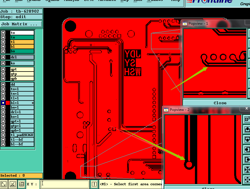
4 Types of PCB Open Circuit
- Repeated open circuit
The repetitive open circuit’s characteristic is that the same open-circuit appears in the same place on almost every PCB board, and the number of the exposed film is the same. The reason is that there is a defect in the same position on the exposure film as the open circuit of the board. In this case, the exposure film must be scrapped, and the AOI detection of the first and last board during exposure must be strengthened to ensure that the first PCB board is correct before exposure.
- The Gap Open Circuit
A gap in a wire characterizes this kind of open circuit, and the remaining line width due to the gap is less than 1/2 of the standard line width or equal to 1/2. The reason for its formation is also due to defects in the exposed film. JHYPCB recommends changing to a new exposure film and strengthening AOI detection during the exposure process.
- Vacuum open circuit
In some areas, multiple wires appear thinner and thinner (tapering); some are open, some are not, but because the wires are too narrow (less than the minimum line width required by the customer), they have to be scrapped. This defect is that the exposure film and the dry film are not in close contact with the PCB manufacturer. There is air in the middle; that is, the vacuum is not right after the exposure table is closed, and the vacuum does not meet the requirements, which causes the wire to change during exposure.
- scratched open circuit
A scratched open circuit’s characteristic is that the traces of the wire scraped by external force can be seen, which also causes the open circuit. Due to improper operation (for example, the wrong method of holding the board during PCB production, etc.) or the machine causes the wire to scratch and forms an open circuit.
Because the causes of defects in the outer layer are complicated, many situations are possible. Still, most of the flaws appear in materials such as copper-clad laminates, film sheets, dry films, or abnormalities in the exposure, development, and etching processes.
Advanced Learning:
- Best PCB Manufacturer In China
- Custom Circuit Board Printing
- Testing & Inspection Methods For PCB And PCBA
- Flying Probe Testing For PCB
- X-Ray Inspection In PCB Assembly
- 10 Tips To Improve PCB Design For Manufacturability


