Introduction
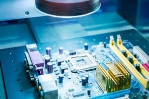
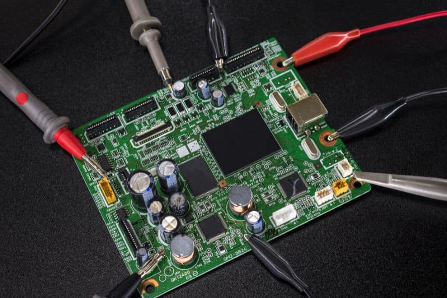
Printed circuit boards are at the heart of electronics. During product development, engineers typically first test concepts by building PCB prototypes before launching into production of PCBs at volume. However, many critical differences exist between prototyping PCBs versus manufacturing PCBs at scale. Understanding these key contrasts is essential for businesses to smoothly transition from design validation to PCB mass production.
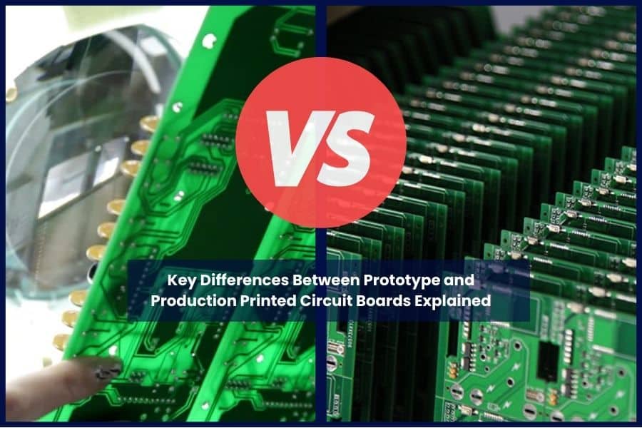
Prototype PCB fabrication refers to producing a small number of PCB boards for functionality testing and concept verification purposes. It focuses on fast turnaround times over shorter production runs. Mass production PCB manufacturing, or production of PCBs, denotes optimizing the printed circuit board design for reliability, quality, and cost efficiencies at high volumes.
This article will explain the vital differences companies should consider across these phases, including contrasts in:
- Lead times and order volumes
- Design iteration flexibility
- Testing requirements
- Fabrication processes
- Cost structures
- Tools and capabilities
Applying insights from this analysis can help hardware teams cost-effectively evaluate designs through prototyping before scaling up production with the right manufacturing partner. It enables enterprises to accelerate the product development life cycle while avoiding pitfalls in taking concepts to mass production.
Table of Contents
PCB Prototyping vs Mass Production: Lead Times and Order Volumes
One major difference between PCB prototyping and production lies in lead times and order quantities.
For PCB prototype fabrication, PCB manufacturers can deliver in very short timeframes, sometimes as fast as 24-48 hours. This enables rapid design iterations and testing early in the development cycle. Typical prototype PCB orders may range from just 5-10 boards for simple proof-of-concept validation.
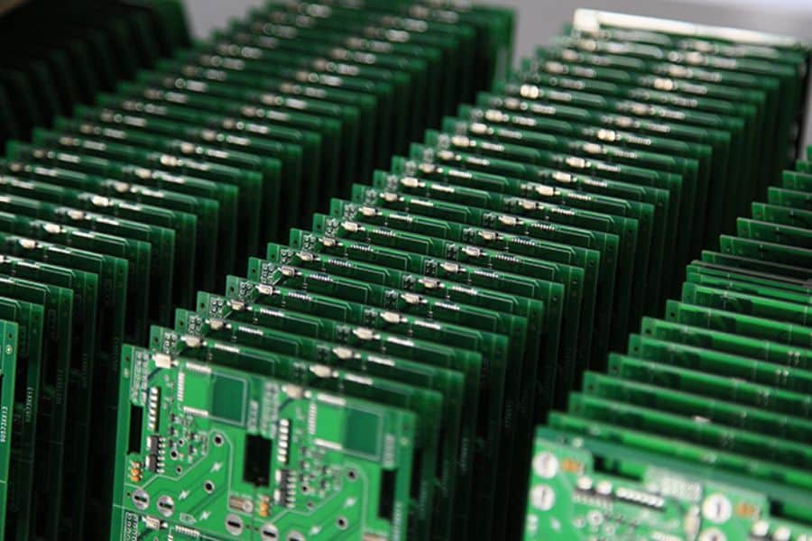
However, production PCB factories are optimized for higher volumes of at least hundreds or thousands of boards. They focus more on process stability, yield improvements, quality assurance, and cost reductions at scale. Thus, on average, PCB production lead times tend to be longer, often 4-6 weeks.
Rushing PCB mass production with very tight deadlines can lead to undue stress on manufacturers’ complex workflow and supply chains. This negatively affects quality consistencies. Savvy hardware teams understand these dynamics and engage their chosen production partners early to forecast volumes and schedule manufacturing runs.
In summary, PCB prototypes prioritize fast turnaround to accelerate innovation, while high-volume production centers on reliability, efficiency, and economies of scale across larger orders. Planning appropriately across these phases is vital.
Design Flexibility: Iteration for Prototypes vs Change Control for Production
Another major contrast comes in the area of design iterations and engineering change orders (ECOs).
With PCB prototyping, the primary goal is evaluating functionality, revealing flaws, and refining the board layout. As such, manufacturers provide more flexibility for designers to prototype PCB layouts and quickly implement modifications freely. Frequent changes are seen as constructive steps to optimize performance before committing to production. This empowers design teams to improve and enhance their boards progressively.
However, once the design moves into volume production of PCBs, excess modifications become very risky and costly. For every incremental layout change, the factory has to redo photomask drawings, potentially scrap components, adjust production processes, and re-verify boards. This unavoidably leads to delays and price markups.
Therefore, manufacturers advise minimizing alterations once mass production is slated to start. Design for manufacturability (DFM) audits performed earlier in the prototyping stage can catch most issues upfront and help enterprises lock down mature layouts before ramping up output. This preventative approach saves time and money compared to reacting to problems through on-the-fly changes down the line after launch.
In essence, PCB prototyping supports relatively easy design tweaks for function validation while disciplined change management is imperative during manufacturing scale-up to control expenses and lead times closely.
Quality Priorities: Functionality Testing for Prototypes vs Stringent Reliability Validation for Production
PCB Prototyping and production phases also differ substantially in quality and reliability validation requirements.
When prototyping new PCB designs, the vital task is proving basic functionality in an economical manner. As long as the concept works reasonably well, engineers can validate design ideas without stringent standards. Quality may be quantified primarily through first-time success rates.
However, releasing products demands far more rigorous quality control and reliability verification through extensive testing. Factories utilize optimized fabrication processes to minimize defects and ensure consistently high yields at volume. Common audits include assessing solderability, circuit integrity, electronic functionality, and environmental stress screening over long durations.
These methodical checks filter out flaws that may otherwise trigger field failures down the road despite initially appearing to work. Such prevention avoids expensive warranty costs and brand reputation damage later.
In short, prototypes focus on preliminary concept verification, while disciplined quality control and reliability assessments safeguard customer experiences during mass deployments.
PCB Materials and Manufacturing: Rapid Techniques for Prototyping vs Advanced Processes for High-Volume Production
Prototyping and production also leverage different PCB materials and fabrication techniques aligned to their respective goals.
To meet urgent deadlines, prototyping emphasizes speedy fabrication. Prototype PCB manufacturers select easier to etch copper types like rolled copper along with more affordable laminates like FR-4. Process steps are optimized for rapid turnaround over superior quality. Standard density interconnects suffice for most early testing needs.
By contrast, volume production PCB fabrication demands repeatable performance, durability, and high yields over elongated operating lifecycles. Thus, mass PCB production adopts higher-grade materials like oxygen-free copper and exotic substrates for specialized applications. Manufacturers fine-tune intricate fabrication processes for precision and stability through advanced automation. Some also offer sophisticated capabilities like HDI, rigid-flex PCBs, and impedance control to suit complex device engineering requirements.
In summary, fast-track simplified methods for prototyping give way to sophisticated, high-precision techniques for predictable manufacturing. Firms get the best outcomes by matching fabrication approaches to their current stage objectives.
Cost Structures: Affordable Prototyping vs Optimized Costs at Scale
Finally, key economic differences also exist between prototypes and production.
For PCB prototyping, unit costs tend to be higher owing to smaller economies of scale. But lower volumes suit early-stage market validation. As long as selected vendors offer competitive prototyping prices, total expenditures stay modest in absolute terms.
Conversely, mass production of PCBs focuses intensely on minimizing per-unit costs by maximizing fabrication yields and utilization rates across high-volume orders. But factories require sizable upfront investments in custom testing rigs, large component inventories, and sophisticated machinery to achieve those low costs ultimately. This demands reliably high forecast volumes and firm commitments through bulk purchase orders once beyond prototyping.
In essence, prototyping emphasizes affordability for preliminary concept verification, while volume production centers on driving down per-unit costs subsequently by scaling up rigorously.
Manufacturing Tools and Capabilities: Flexible Prototyping vs Automated High-Precision Production
Prototyping and production also utilize quite different manufacturing infrastructures and capabilities.
For quick-turn prototypes, manufacturers adopt modular tooling like laser direct imaging (LDI) that allows rapid design revisions. Smaller equipment facilitates fast fabrication of limited quantities. But tradeoffs result in reduced placement accuracy or reliability over mass production.
Whereas dedicated mass production relies on fixed, precise tools like advanced multi-head automated pick-and-place equipment. Mature smart factories also implement sophisticated testing, inspection, and quality assurance regimes to guarantee reliability, efficiency and yields while minimizing defects. These capabilities require thorough planning and sizable capital expenditure ahead of manufacturing at scale.
In short, nimble prototyping tools quickly validate concepts, while methodical mass production environments ensure predictable quality outputs across high volumes. Companies are advised to test ideas economically through rapid prototyping first before transitioning to automated, large-scale fabrication workflows.
Frequently Asked Questions
A PCB prototype is a small batch of printed circuit boards built for the purpose of testing and validating a new design before committing to full production. It allows engineers to verify functionality, identify issues, and refine the layout.
PCB prototyping is crucial as it enables rapid design iterations and concept verification early in the development cycle. This prevents costly mistakes and reworks further down the line during PCB mass manufacturing.
Prototype PCBs typically use more economical materials like rolled copper and FR-4 laminates to reduce costs during the initial testing stages.
The main advantages of building PCB prototypes include:
- Rapid Design Validation: Prototypes enable quickly proving out new PCB concepts and architectures early in the development cycle before high costs are incurred.
- Uncover Design Flaws: Building physical prototypes helps reveal potential issues with component placement, routing, thermal management, and more that may not be apparent in simulations.
- Iterate Quickly: The prototyping stage allows designers to easily make changes and refine the board layout based on testing feedback.
- Reduce Development Costs: By identifying and resolving problems early through prototyping, companies can avoid expensive reworks and delays later during high-volume manufacturing.
- Accelerate Time-to-Market: The ability to quickly validate PCB designs through iterative prototypes helps complete final production-ready boards sooner.
So, in summary, leveraging PCB prototypes facilitates de-risking new product designs, implementing changes cost-effectively, and accelerating the overall development cycle prior to scale-up.
A rapid PCB prototyping service refers to the capability offered by some PCB manufacturers to produce small batches of prototype boards with extremely fast turnaround times, sometimes within 24-48 hours. This allows for an accelerated prototyping and iteration cycle during product development.
The key features of a rapid prototyping service include:
- Quick-turn manufacturing – Utilizing optimized processes and reserved capacity to fabricate prototypes rapidly.
- Small batch quantities – Offering low minimum order quantities, sometimes as low as 1-5 boards per order.
- Simple ordering – Easy file uploads and online ordering without need for complex procurement processes.
- Low NRE costs – No or minimal upfront non-recurring engineering charges.
- Design flexibility – Accommodating late engineering changes with fast respins.
By leveraging a rapid PCB prototyping service, hardware companies can validate designs, test functionality, and implement iterations at an unprecedented speed compared to traditional prototyping methods. This accelerates the overall product development timeline significantly.
PCB Prototype fabricators can produce small batches extremely quickly, sometimes within 24-48 hours using rapid PCB prototyping services.
PCB prototyping is a crucial step but not every production run requires going through prototype proofing. The key circumstances where prototyping is recommended include:
- New PCB Design Projects: When developing a brand new printed circuit board design, prototyping should be performed to validate the layout, test functionality, and uncover any issues before high-volume manufacturing.
- Design Updates/Revisions: If an existing PCB design undergoes changes or upgrades, prototyping the updated board is advisable to ensure the modifications work as expected.
However, prototyping may not be needed for established designs that are already being successfully produced in batches with no changes required.
JHYPCB offers rapid PCB prototyping services for double-layer, 4-layer, 6-layer and 8-layer PCBs. For PCB prototypes, FR-4 and aluminum materials are typically recommended to balance cost and performance. Our team follows rigorous standards to deliver high-quality PCB prototypes rapidly. Once PCB prototyping is completed satisfactorily, additional production PCBs with various materials and layer counts can be ordered.
PCB prototyping allows you to verify your PCB design thoroughly before committing to a full production run, saving time and costs by identifying potential issues upfront. It’s a wise investment for new products and design iterations.
Rapid PCB prototyping services are able to provide extremely quick turnaround times, sometimes within 24-48 hours, by utilizing specialized processes and capabilities:
- Optimized Prototype Production Line – These services have dedicated production lines focused solely on quickly manufacturing small prototype batches, rather than large high-volume runs.
- Rapid Setup and Changeovers – They use flexible tooling like direct imaging, allowing fast machine setups and changeovers between prototype jobs.
- On-Demand Manufacturing Model – Prototype production happens on-demand as orders arrive rather than based on batched schedules.
- Prioritized Order Handling – Prototype orders get prioritized through specialработа queuing processes ahead of larger production orders.
- Automated Order Processing – Order entry, file checks, and quality processes are highly automated to reduce human delays.
- Reserved Capacity – A portion of the factory’s manufacturing capacity is always reserved for rapid prototyping.
- Quick-Turn Material Stocking – Common prototype materials are stocked in high volume ready for immediate use.
By streamlining and optimizing processes specifically for low volumes and rapid cycles, PCB prototype manufacturers can reliably produce quality boards in remarkably short timeframes to accelerate product development cycles.
When preparing to build PCB prototypes, there are several key requirements to have in place:
- PCB Design Files: You’ll need to provide the PCB manufacturer with your complete design files, including the Gerber files, drill files, BOM file, etc. The design files should be thoroughly checked for any issues.
- Bill of Materials (BOM): Have a comprehensive BOM specifying all the required components for the prototype boards, including part numbers, package types, quantities etc.
- PCB Stack-up Details: Provide the layer stack information, materials, finishes and any special requirements for the prototype boards.
- Design Rules/Constraints: Share your design rules like spacing, trace widths, hole sizes and any electrical constraints that need to be adhered to.
- Test Requirements: Clearly define what types of tests (electrical, environmental, etc.) you plan to perform on the prototypes and any test fixtures/aids needed.
- Sample References (Optional): If available, provide sample boards or components to ensure prototypes match existing references exactly.
The more complete and accurate the information provided upfront, the smoother the prototyping process will be. Clear requirements help reduce revisions and get prototypes built faster for design verification.
Additionally, manufacturers may request order details like quantities, turnaround times, special packaging needs and shipping instructions to properly fulfill the prototype order.
To submit a prototype PCB design or request a quote, it’s important to provide your PCB manufacturer with detailed specifications about your board requirements. The more information you can include upfront, the better to ensure your PCB prototypes are built exactly as intended. Here are some key details to have ready:
- Number of layers required
- Board thickness/material
- Board dimensions/size
- Copper weight/thickness
- Minimum trace width/spacing
- Minimum hole/via size
- Minimum annular ring
- Surface finish type (ENIG, HASL, etc.)
- Solder mask color
- Silkscreen legend colors
- Drill files (NC Excellon format)
- Drill tool list file
Additionally, you’ll need to supply your complete Gerber file set and any other design files like ODB++, pick-and-place files, etc. Providing comprehensive design data upfront allows the manufacturer to quote and build your prototypes to specifications accurately.
Clear requirements help avoid issues, reduce tolerances, and accelerate your prototyping cycle. The more detail you can provide, the smoother the PCB prototype manufacturing process will be.
Mass production PCB manufacturing typically involves volumes of at least hundreds or thousands of boards to achieve economies of scale.
Key cost drivers include the board complexity, chosen materials, required certifications, production volumes, and manufacturing setup costs.
Robust quality control through stringent DFM audits, standardized processes, environmental stress testing, automated inspection and more.
While varying by project, 4-6 weeks is a common average lead time for volume PCB production after placing an order with the manufacturer.
Conclusion and Takeaways
In conclusion, understanding the critical differences highlighted in this article between prototype PCB fabrication and volume PCB manufacturing enables organizations to set the right expectations when transitioning between these phases.
The prototyping stage allows fast iterations for design experimentation and concept verification on a budget. Afterwards, mass production requires increased planning and coordination with manufacturing partners on specifications, quality protocols, volumes and timelines to control costs and lead times during scale-up.
As one of China’s leading PCB manufacturers, JHYPCB has supported the complete product realization journey for numerous customers globally. Our specialized services range from 24-hour quick-turn prototype boards to facilitate design validation all the way through to high-quality mass production runs along with complete PCB assembly solutions.
We urge engineering teams to leverage capable suppliers possessing expertise across low, medium, and high-volume PCB production scenarios so product development cycles can be shortened dramatically while avoiding manufacturing pitfalls as innovative devices progress towards commercialization.
Contact us at sales@pcbjhy.com to explore how our comprehensive prototyping and manufacturing capabilities can accelerate your next electronics project.
Related Reading