In the printed circuit board (PCB) design (PCB Layout), we will consider the following questions: design for how many layers of PCB?Single-sided PCB?Double-sided PCB?Multilayer PCB?ESD / EMI how to protect? Is the assembly and soldering process of the circuit board single-sided or double-sided? Should the electronic parts be full of through-hole inserts or full SMD chips? Or SMD+insert?
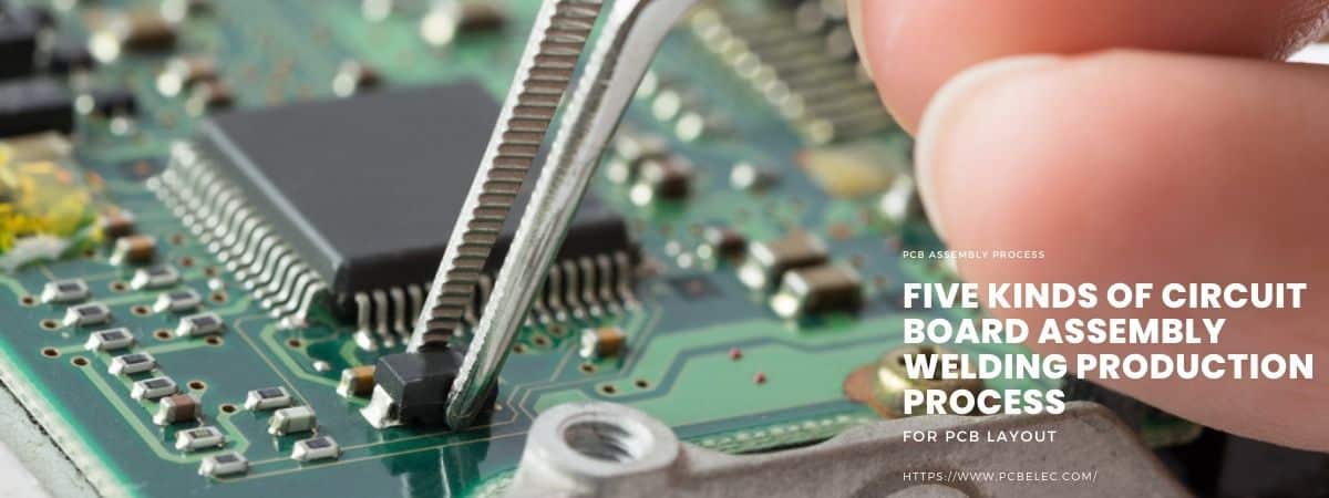
This article will focus on the soldering production process for circuit boards.
1. Single-layer PCB?Double-sided PCB or Multilayer PCB?
More PCB layers mean more circuits can be carried on the same surface area, and the layers are connected with vias.
The more layers of PCB usually mean that the smaller the PCB size can be designed with more features, but the production cost is relatively more expensive.
Usually, the more advanced the board, the more layers there will be at least one ground layer and power layer.
2. Single-sided welding or double-sided welding?
The type of PCB is related to the production cost of assembled circuit boards. If possible, try to put all parts on only one side of the board (the same side), significantly reducing the production process. It is important to know that even if there is only one part on the other side of the board, it is still generally necessary to have an additional soldering process. If you can move the part to the same side as the other parts, you can reduce the cost of one production line.
3. PCB assembly process: all PTH, all SMD, or PTH + SMD?
If you can do all through-hole PCB assembly (wave soldering process) or all SMD (SMT process) is best. This will not require an additional production line; SMT and wave soldering belong to different welding processes. And now the EMS manufacturers have less and less use wave soldering. Suppose you can avoid the wave soldering process. In that case, you should avoid it because wave soldering requires the wave soldering furnace to be heated beforehand, and the electricity cost to heat the whole furnace to the melting temperature is high enough.
4. Does the SMT factory support the red glue wave soldering process?
The red glue process is not available in every EMS manufacturer, so it needs to be clearly confirmed before the design so that it cannot be put into production after the design.
Secondly, the wave soldering and reflow soldering processes will have different pad distance and size design requirements for the same electronic part. It is recommended to consult the SMT manufacturer first and obtain the relevant DFM requirements.
5. How do EMS or SMT manufacturers calculate PCBA costs?
Most EMS (Electronics Manufacturing Service) or SMT manufacturers calculate the foundry cost by labor hours. A few manufacturers calculate the processing cost by a certain percentage of the material cost of the BOM, and all the fixture costs will also be calculated within the cost.
If the PCB assembly uses both SMT and waves soldering process, generally speaking, the cost of SMT unit labor hours will be more expensive than wave soldering because SMT equipment is more expensive, and SMT operator quality requirements are higher, so the relative salary will also be higher.
In principle, if you can reduce the processes, then you can save production costs. This is because the basic cost of opening a whole production line at the same time is the same whether only one-tenth or one-half of a production line is used, and it will not be reduced the cost by using less.
6. common PCB assembly process
6.1 Circuit Board Assembly Process Option 1: Single-sided PCB full-through-hole assembly - wave soldering process
Process: single-sided through hole PCB assembly-wave soldering
Single-sided PCB wave soldering refers to the electronic parts (insert parts or through-hole parts), including resistors, capacitors, and inductors. Manual inserts insert parts into a single-sided board and flow-through wave soldering to solder the parts to the circuit board. The characteristic of this kind of PCB board is that the parts are all on the same side of the circuit board so that the parts can be soldered after only one wave soldering.
In the early days, when there were no SMD parts, almost all circuit board assembly used this process. The disadvantage is that it requires more board space, and as technology has evolved, many parts have been converted to SMD, so it is rare to see this assembly process now.
Now occasionally, you can see that some cheap power supplies or transformers or mouse boards still use this process because the parts are cheap or because parts that can withstand high current or voltage are needed; if you still use SMD, the cost will be significantly increased, and most boards still use low-cost paper circuit boards. Some unique boards need to use parts that can withstand high current or voltage. SMD parts may not replace such parts.
6.2 Circuit board soldering process option 2: single-sided PCB SMT+wave soldering process
Process: single-sided solder paste printing-SMD-reflow-single-sided through-hole assembly-wave soldering
This circuit board soldering process is generally also suitable for single-sided circuit boards. SMD and through-hole parts are placed on the same side of the circuit board. In the process, the board is printed with solder paste through the SMT line, and the SMD parts are placed on the board. The SMD parts are soldered to the board by reflow soldering. Then the through-hole components are inserted into the board manually or by an auto component inserter through a through-hole component assembly station. Then the through-hole components are soldered to the board through wave soldering.
Because the size of PCB boards is getting smaller and smaller, and SMD parts are becoming more and more popular and cheaper, most of the assembly processes of consumer circuit boards have now developed to “SMD+DIP.” That is to say, most of the electronic components on the assembled circuit boards are packaged with SMD, and a small number of components that SMD cannot replace are used, or through-hole inserts are used based on price considerations.
Therefore, this is also the most cost-effective circuit board assembly process at present.
6.3 Circuit board welding process option 3: double-sided PCB double-sided SMT + red glue + wave soldering process
Process: printing solder paste on the first side – placing SMD parts – 1st reflow – red glue on the second side – placing SMD parts – 2ed reflow – inserting on the first side – wave soldering
This is an earlier process for assembling double-sided circuit boards. Early electronic components are still in the stage of transitioning from through-hole components to SMD component packaging. There will be at least 10 traditional through-hole components or more on a circuit board. Moreover, the small chips such as resistors, capacitors, and inductors were still above 0603, and some even used 1206.
Therefore, there is red glue on the second side of the PCB board to fix the SMD parts, and then the wave soldering process is performed after the through-hole components are inserted. Because both solutions 1 and 2 can only install electronic components on a single-sided circuit board, if the components can be placed on the second side of the board, the utilization rate of the board can be significantly increased. However, if the solder paste printed on the second side of the board is soldered and then used for wave soldering, because there are still many through-hole components on the board, the solidified solder paste on the second side will be melted when it passes through the wave soldering furnace. The electronic parts on the surface will fall into the tin pool, so the red glue process was developed. Red glue is generally an irreversible epoxy resin material that can stick to SMD parts and will not re-melt even when passed through a wave soldering furnace.
Restrictions of usage:
a. Not all SMD parts can be wave soldered with red glue, only some IC parts with double-row pins extending outwards or parts with pads at both ends (such as small chips such as resistors, capacitors, inductors, etc.) can be Use the wave soldering process.
b. ICs such as QFP with outstretched pins on all four sides can also be wave soldered, but the pin spacing must be large enough; otherwise, short circuits are prone to occur.
c. In addition, 0603 is almost the minimum limit of the current red glue process. If the size is too small, the red glue will cause empty soldering because red glue is not as easy to control as solder paste. In addition, if the spacing between the pads is too small, it is easy to cause a short circuit during wave soldering.
6.4 Circuit board soldering process option 4: double-sided PCB double-sided SMT + through-hole components selective wave soldering process
Process: first side printing solder paste-SMD-1st reflow-second side printing solder paste-SMD-2nd reflow-through-hole components inserting-selective wave soldering or carrier wave soldering
With the progress of the times, this double-sided SMT manufacturing process can be regarded as the most common design because most electronic parts can already be found in SMD packages, and only a few are left to withstand external forces. Based on functional and reliability considerations, the IO connector used through-hole inserts to ensure that rude people would not break its soldering
This circuit board assembly process has abandoned the red glue process. For the few parts that still need to be soldered by the wave soldering process, consider using a wave soldering mask carrier or tray to cover the parts that have been soldered in SMT, and then only expose the pin positions of the parts that need to be wave soldered.
In addition, it is also possible to consider the introduction of the more popular selective wave soldering furnace equipment, which uses a small tin furnace and nozzle and adopts automatic computer control to solder through-hole parts from the bottom.
However, the soldering process of the above two through-hole components requires a keep-out area, and please refer to the DFM requirements when designing.
In addition to the above two wave soldering, because there are not many through-hole components, some people will use some cheaper processes:
a. Hand soldering: We do not recommend hand soldering because the quality is difficult to control, false soldering and empty soldering often occur at the ground pins, and parts with fine pitch pins are a test of skill and vision, requiring highly skilled workers and long-term Welding work is also detrimental to the health of welders.
b. Robotic-arm or automatic welding equipment: Automatic welding can be cheap or expensive. This type of equipment generally still uses soldering iron and tin wire, just let the machine replace manual welding, and can be achieved by using a simple XYZ three-axis or more table. Still, the precision and parameters require a long time to debug.
There is also a through-hole reflow (PIH, PASTE-IN-HOLE) process. Although it also has through-hole components, after the heat resistance level of the material is improved, the through-hole components can be used as SMD parts for SMT and reflow. Direct welding after the furnace eliminates subsequent welding of through-hole components.
6.5 Circuit board welding process option 5: double-sided PCB board full double-sided SMT process
Process: printing solder paste on the first side-SMD-1st reflow-printing solder paste on the second side-SMD-2nd reflow
At present, almost all smartphones and some consumer electronic products use this process because today’s smartphones almost have a Type-c or Lighting IO connector left.


