Knowing how to verify the quality of PCB has become crucial because a printed circuit board that is not properly designed has a has high chance of not working as it ought to. Also, this is important because a company can claim to be an expert in the design and manufacture of PCBs. However, in the real sense, they are nothing but flops. If you don’t want to waste your time and money collaborating with the wrong PCB manufacturers, then you must be extremely good at telling the difference between high-quality printed circuit boards and those that are poorly designed.
The major aim of this article is to reveal seven ways you can use in telling the quality of a printed circuit board. We will run through the procedures one after the other, and choose anyone for yourself thereafter.

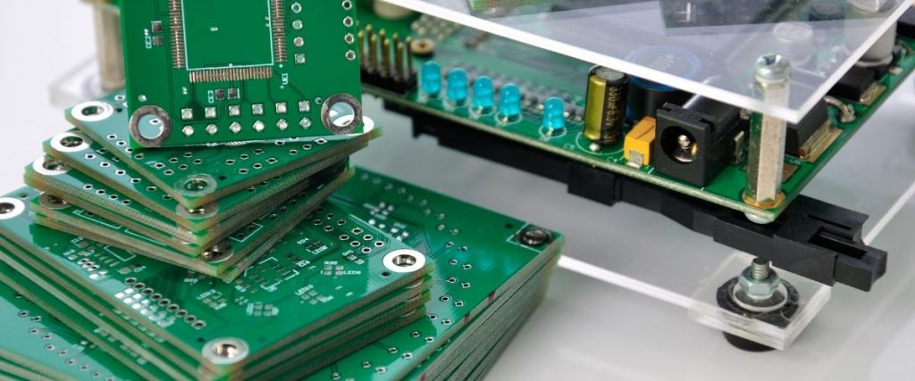
7 Ways to Judge PCB Quality
#1-PCB Traces
You can start by looking at the PCB traces. This is expected to contain a solder mask layer that will prevent the copper on the board from experiencing shorts or oxidation. The solder mask can be of various colours. The white colour solder mask can make it difficult for the traces to be seen. That is why the green solder mask is mostly preferred.
Also, check to see if all the traces are in a straight line, devoid of any bends. That is because bent lines could reduce the efficiency of such boards for high power & high-efficiency applications. You have to be extremely sure before you can accept PCBs with any kind of bends.
#2-Decoupling Capacitors
This is one component that is easily overlooked on the printed circuit board. All the chips on a PCB are powered. But not too many people take time to consider the distance between those chips and the sources where they get their power from. In such instances, power is normally directed towards the chip through PCB traces.
Decoupling capacitors don’t need to be far from the chips because they help to cancel out any high-frequency interference that could impact the performance of the chip negatively. The general rule of thumb is that when a chip has multiple VDD pins, each of those pins would need at least one decoupling capacitor.
The ideal thing is to have the decoupling capacitors placed close to the chip pins. Failure to do this will result in a drop in the efficiency of the chip and the PCB in general. So, always check the distance between the decoupling capacitors and their chip pins.
A quick tip is, when the decoupling capacitors are not by the side of their chip, it goes without mentioning that such board designs have not to be done correctly.
#3-Length of PCB Traces
The length of all the PCB traces should be the same, especially for designs that require that the relationship between multiple signals be timed. For instance, this is key when directing a high-speed clock signal to several chips or the address bus and data lines running between the RAM memory and microprocessor.
This is done to ensure that every signal arrives their destinations with the same delays, thereby preserving how the signal edges relate with one another.
#4-Antenna Feedlines
If your PCB design comprises a transmitter, receiver, or transceiver, an antenna would be needed. For optimal performance, the feedline existing between the RF Chip’s pin should be matched to the connected feedline in terms of impedance. The feedline should be equal to the antenna’s impedance. The main reason why there has to be impedance matching is for maximum power transfer to be achieved between the radio chip and antenna. A mismatch can easily result in a drop in power transfer, negatively influencing the operating range.
#5-Component Placement
Interestingly, decoupling capacitors are not the only components that are expected to be placed strategically on the printed circuit board. There are conditions that surround how other components should be placed as well.
For example, if your PCB is going to house inductors, then the standard is that they don’t stay too close to one another. The reason being that inductors set up a magnetic field. Therefore, whenever they are placed too close to one another, it might result to unwanted coupling. Secondly, these inductors should not be kept close to metals of any type. Induced currents can be formed on the metallic objects by the inductors, which could lead to a change in the inductors’ value.
That said, the donut-shaped, toroidal inductors are not culprits when it comes to producing unwanted magnetic fields. So, if that is the kind of inductors on your PCB, you may disregard their placement. All components on a PCB should be put in sections according to what they can deliver.
#6-Trace Width & Routing
The size of the traces is not done anyhow. Traces accommodating high currents are to be sized correctly. There is a standard as regards how this should be done. There are different trace widths that are approved for different currents. Traces with small analogue signals can run parallel to the ones carrying fast-changing or digital signals.
Traces that connect inductors should not be wider than recommended. That is because such can easily give rise to radio frequency emissions that would negate the board’s performance. Check online for more details on this.
#7-Grounds & Ground Planes
For PCBs that are moderately complex, the best thing is using a 4-layer board where the 2 layers inside will act as the supply & ground plane.
If the PCB design comprises a mixture of analogue and digital sections, splitting of the ground plane will be necessary, and can be joined at the negative terminal of the power supply. This helps to prevent current spikes in ground current from the digital side that can damage the analogue section.
How to ensure PCB quality?
We have described seven methods for judging the quality of PCB boards above, and then we will discuss the methods of PCB quality control.
The final test and inspection do not determine the quality of the PCB. Still, it requires effective management and monitoring in PCB design, PCB manufacturing and PCB inspection.
Quality Control in PCB Design
To ensure the quality of PCB design, you need to ensure the following three aspects.
- Ensure the correctness of the PCB design files
- Ensure the manufacturability of the PCB
- Ensure the standardisation and standardisation of PCB design
- Ensure the testability of the PCB
Quality Control in PCB Manufacturing
- Make sure you find the proper PCB manufacturer
- Ensure the capability of the PCB manufacturer
- Ensure that the PCB complies with IPC standards and RoHS, and other legal and regulatory requirements
- Make sure to check and confirm before PCB manufacturing
- Ensure the quality of critical links in PCB manufacturing
- Make sure to operate in strict accordance with the operation instructions
Quality Control in PCB Testing
PCB inspection is the last link in PCB quality control. It is necessary to test the PCB quality strictly according to the inspection methods through visual inspection or special equipment. PCB and PCBA testing and inspection methods are as follows:
- In-Circuit Testing (ICT)
- Flying Probe Testing
- Automated Optical Inspection (AOI)
- Burn-in Testing
- X-ray Inspection
- Functional Testing
- Other Functional Testing
- Soldering Test
- PCB Contamination Testing
- Micro-sectioning Analysis
- Time-domain Reflectometer (TDR)
- Peel Test
- Solder Float Test
- Interconnect StressTest (IST)
Conclusion
Whether you intend to design your PCB yourself or give the job out to someone else, it is important that you can identify a PCB with good quality and the one that isn’t. The above tips can be very helpful to you in this regard.
Related Reading
- 30 Common SMT PCB Assembly Defects
- Quality Control of Engineering Data for Multilayer PCB
- Angle Control in Multilayer PCB
- IPC Standards: A Guide to Standards for PCB Manufacturing and Assembly
- What Does PCB Open Circuit Mean?
- Why Should PCB Reliability Be Taken Seriously?
- Testing & Inspection Methods For PCB And PCBA
- Flying Probe Testing For PCB
- X-Ray Inspection In PCB Assembly


