"An engineer who does not understand PCB manufacturability design cannot have a good PCB design."
PCBELEC.COM
PCB Design ≠ PCB Manufacturing
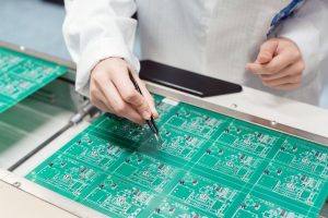
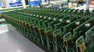
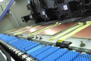
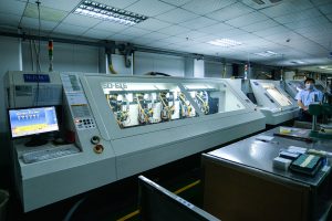
In the electronics industry, the quality and reliability of products depend primarily on the manufacturer’s process capabilities. The PCB factory is not a black box production line. It’s not that you give them the relevant PCB design data, and you can get a finished product that is precisely the same as the PCB design after a few days.
PCB design is a complete and rigorous process system, and PCB manufacturing is another set of sophisticated production and processing systems. At the same time, PCB design data is not equivalent to PCB manufacturing data. In other words, PCB manufacturing does not directly use PCB design data. PCB design data needs to be converted into production data for machines through CAM (Computer-Aided Manufacturing).
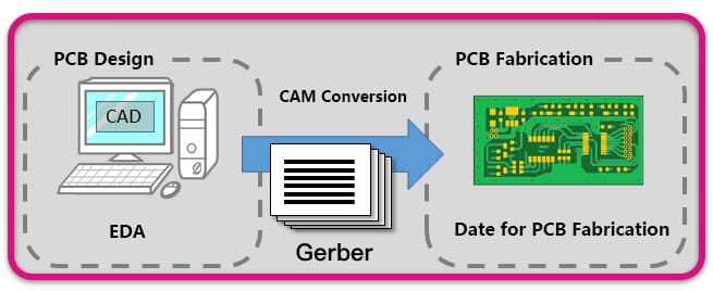
PCB Designers Need to Understand the PCB Manufacturing Process
Suppose the PCB designer does not understand the PCB manufacturing process and the CAM data conversion process, or the CAM engineer does not understand the relevant terminology of PCB design. In these cases, there will be problems in the data conversion from PCB design to PCB manufacturing.
Especially for “low-level” format files, like Gerber, that describe a single image, you also need an additional description file to describe your PCB manufacturing requirements, such as impedance control, layered structure, surface finish, and so on.
The information used for PCB manufacturing can be placed in an additional Gerber file, or it can be placed in a document file like Word for description in graphic form. However, where there is a text description, there will be problems with expressing and understanding the information; it is necessary to use telephone, email, or other communication tools to communicate and confirm. Suppose both parties use their professional terms to describe the problem and cannot clearly understand it. In that case, they all think that the other party does not know everything, and low-efficiency or even wrong communication is often the culprit for PCB manufacturing failures.
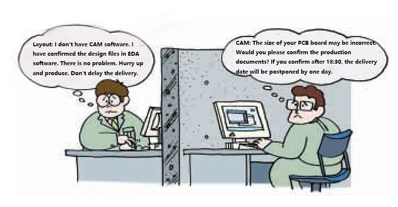
Why PCB Manufacturability Inspection and Analysis?
As a qualified and excellent PCB designer, a designer/engineer will try his best to avoid leaving the problem to the PCB manufacturer. Before submitting the manufacturing data, the PCB designer should check it in the CAM. He needs to check the design from the perspective of the PCB manufacturer during layout and adjust the PCB Layout design according to the process capabilities of different PCB manufacturers. This process is DFM (Design For Manufacturing). It requires us to understand the manufacturing process, production process, board performance, etc., of the cooperating PCB factory while designing the PCB.
You might think, why do you want to layout from the perspective of a PCB board manufacturer? It is not to increase the workload for ourselves, nor reduce the workload of the CAM engineers of PCB manufacturers. It is because we want the printed circuit boards produced by PCB factories to be qualified products. Suppose the product is defective due to errors in the design documents or manufacturing information. In that case, the final impact will delay the progress of our project, and we will still suffer the loss.
It Would Be Best If You Had a Helpful PCB DFM Tool
The function of CAM software is very powerful, which is very suitable for professional CAM engineers of PCB factories to output production data. However, for PCB designers, using CAM software will virtually increase their learning costs.
We avoid manufacturability risks by adding DFM design rules in the EDA design software when doing PCB design. After exporting the manufacturing data, perform a self-check on the integrity of the manufacturing data. We only need a portable and straightforward DFM tool at this time instead of learning how to use the CAM software.
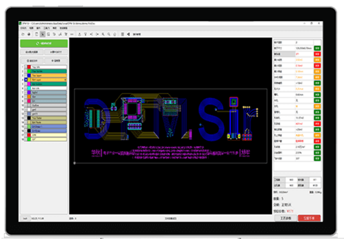
HuaQiu DFM - It is a PCB Design Assistant That Knows More About You
A good DFM tool must be a bridge between design and production, making PCB manufacturing easier.
HuaQiu DFM, a free and easy-to-use PCB manufacturability design analysis software and PCB online inspection tool, can help engineers find design problems and solve problems as early as possible before production. It improves product quality and production efficiency and shortens the product development cycle. It also improves the competitiveness of enterprises.
HuaQiu DFM is an essential desktop tool for PCB engineers, hardware engineers, PCB factories, SMT factories, and PCB traders.
1. Supports the analysis and import of Allegro, Altium, Protel, PADS, ODB, Gerber, and other format files.

2. One-click automatic analysis of design hazards eliminates production difficulties and design defects and prevents quality defects.
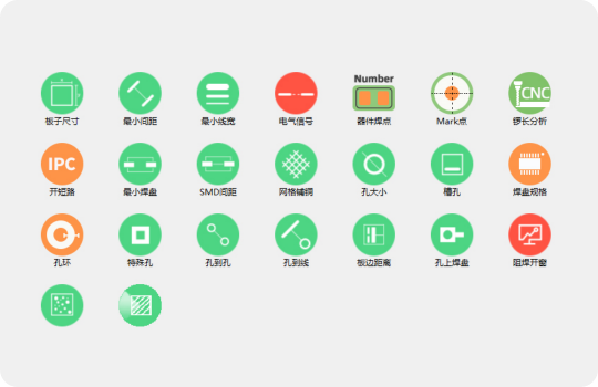
3. Manufacturing analysis of more than 23 items, the higher the score, the more standardized the design
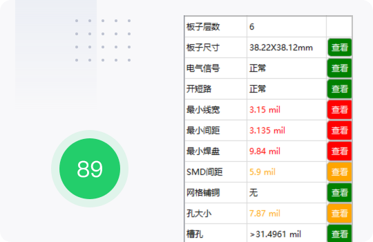
4. Accurately locate the location of the problem and give the most reasonable optimization suggestions and solutions for the problem.
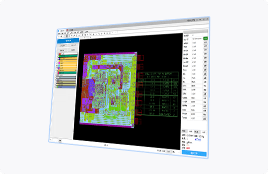
5. Integrate multiple innovative tools to eliminate tedious operation links and achieve efficient work.
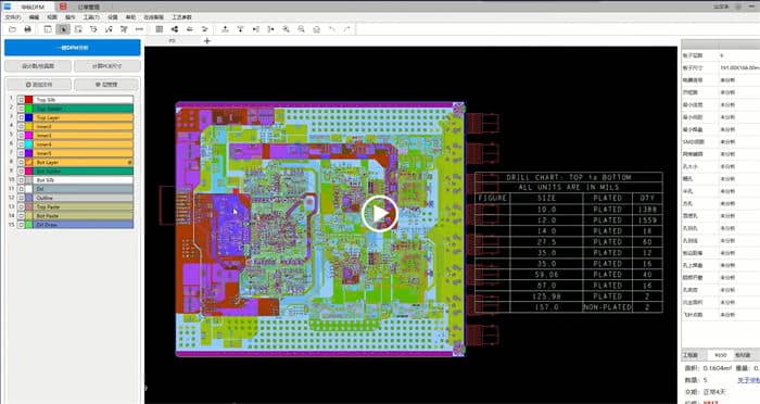
6. Automatically match the PCB stacking structure in line with the production, making the quality of the multi-layer PCB more reliable
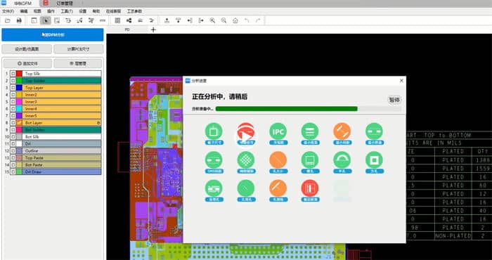
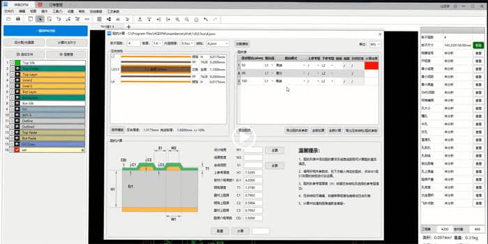
7. Combining various production factors, automatically calculate or inverse impedance
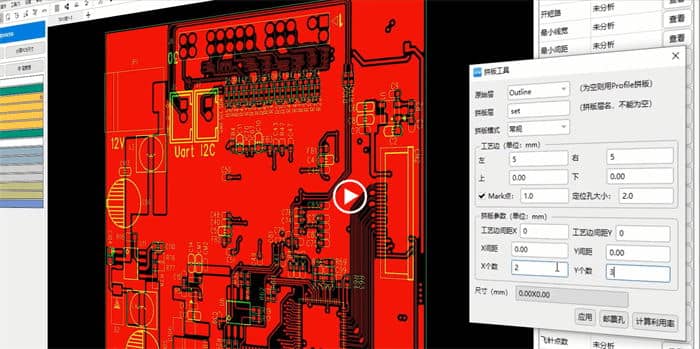
8. Check whether the parameters of the component are correct, and replace the complicated operation of Excel
Online inspection and APP download
You can also click here to download the App.
Read more
- Basic Knowledge of PCB Pad Design
- 10 Tips To Improve PCB Design For Manufacturability
- HDI PCB Layout and Basic HDI Design Guidelines
- PCB Terminology Glossary
- PCB Design Software Free Download
- Five factors that FPC PCB designers should know about impedance control
- What are the aspects of PCB Design For Manufacturing (DFM) and Design For Assembly (DFA)?
- 4 Solutions to Reduce EMC in 6-layer PCB Design
- DFM And DFA
- Fast Turn Prototype PCB Service


